
Microchip Technology Inc
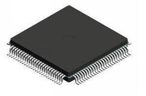
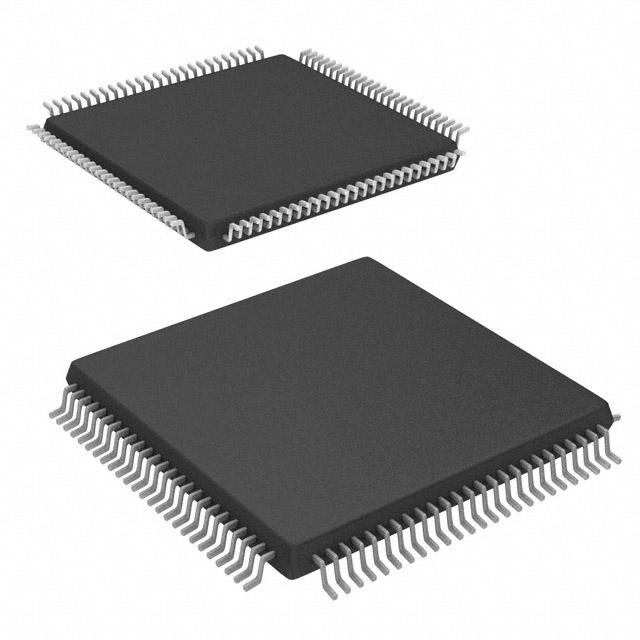
A54SX16P-1VQG100
A54SX16P-1VQG100 ECAD Model
A54SX16P-1VQG100 Attributes
| Type | Description | Select |
|---|---|---|
| Pbfree Code | Yes | |
| Rohs Code | Yes | |
| Part Life Cycle Code | Transferred | |
| Supply Voltage-Nom | 3.3 V | |
| Number of Inputs | 81 | |
| Number of Outputs | 81 | |
| Number of Logic Cells | 1452 | |
| Number of Equivalent Gates | 16000 | |
| Number of CLBs | 1452 | |
| Combinatorial Delay of a CLB-Max | 800 ps | |
| Programmable Logic Type | FIELD PROGRAMMABLE GATE ARRAY | |
| Temperature Grade | COMMERCIAL | |
| Package Shape | SQUARE | |
| Technology | CMOS | |
| Organization | 1452 CLBS, 16000 GATES | |
| Additional Feature | CAN ALSO BE OPERATED AT 5V; 24000 SYSTEM GATES ALSO AVAILABLE | |
| Clock Frequency-Max | 280 MHz | |
| Power Supplies | 3.3,3.3/5 V | |
| Supply Voltage-Max | 3.6 V | |
| Supply Voltage-Min | 3 V | |
| JESD-30 Code | S-PQFP-G100 | |
| Qualification Status | Not Qualified | |
| JESD-609 Code | e3 | |
| Moisture Sensitivity Level | 3 | |
| Operating Temperature-Max | 70 °C | |
| Number of Terminals | 100 | |
| Package Body Material | PLASTIC/EPOXY | |
| Package Code | TFQFP | |
| Package Equivalence Code | TQFP100,.63SQ | |
| Package Shape | SQUARE | |
| Package Style | FLATPACK, THIN PROFILE, FINE PITCH | |
| Surface Mount | YES | |
| Terminal Finish | MATTE TIN | |
| Terminal Form | GULL WING | |
| Terminal Pitch | 500 µm | |
| Terminal Position | QUAD | |
| Width | 14 mm | |
| Length | 14 mm | |
| Seated Height-Max | 1.2 mm | |
| Ihs Manufacturer | MICROSEMI SOC PRODUCTS GROUP | |
| Part Package Code | QFP | |
| Package Description | TFQFP, TQFP100,.63SQ | |
| Pin Count | 100 | |
| Reach Compliance Code | compliant | |
| HTS Code | 8542.39.00.01 |
A54SX16P-1VQG100 Datasheet Download
A54SX16P-1VQG100 Overview
The A54SX16P-1VQG100 is a Field Programmable Gate Array (FPGA) chip manufactured by Xilinx. It is a 16-bit device with a maximum operating frequency of 100MHz. The device contains 54,400 logic elements, 1,200 Kbits of block RAM, and 1,024 I/O pins. It has a power dissipation of 2.3W and an operating temperature range of -40 to 85 degrees Celsius.
The A54SX16P-1VQG100 is suitable for a variety of applications, including high-speed networking, embedded systems, video processing, and digital signal processing. It is also suitable for applications in which a high degree of flexibility is required, such as prototyping, custom logic design, and algorithm development.
The device is programmable using the Xilinx Vivado Design Suite, which provides a complete suite of tools for designing and debugging FPGA designs. The Vivado Design Suite includes a graphical user interface and a powerful set of design and verification tools. It also includes an IP library with a wide range of pre-verified IP cores, as well as support for Open Source development tools such as the GNU Compiler Collection (GCC).
The A54SX16P-1VQG100 is designed to meet the requirements of a wide range of applications, including high-speed networking, embedded systems, video processing, and digital signal processing. It is an ideal choice for designers looking for a high-performance and cost-effective solution.
You May Also Be Interested In
1,639 In Stock
Pricing (USD)
| QTY | Unit Price | Ext Price |
|---|---|---|
| 1+ | $128.7069 | $128.7069 |
| 10+ | $127.3229 | $1,273.2292 |
| 100+ | $120.4032 | $12,040.3198 |
| 1000+ | $113.4835 | $56,741.7368 |
| 10000+ | $103.7959 | $103,795.8600 |
| The price is for reference only, please refer to the actual quotation! | ||