
Microchip Technology Inc
A54SX16A-2TQG144I
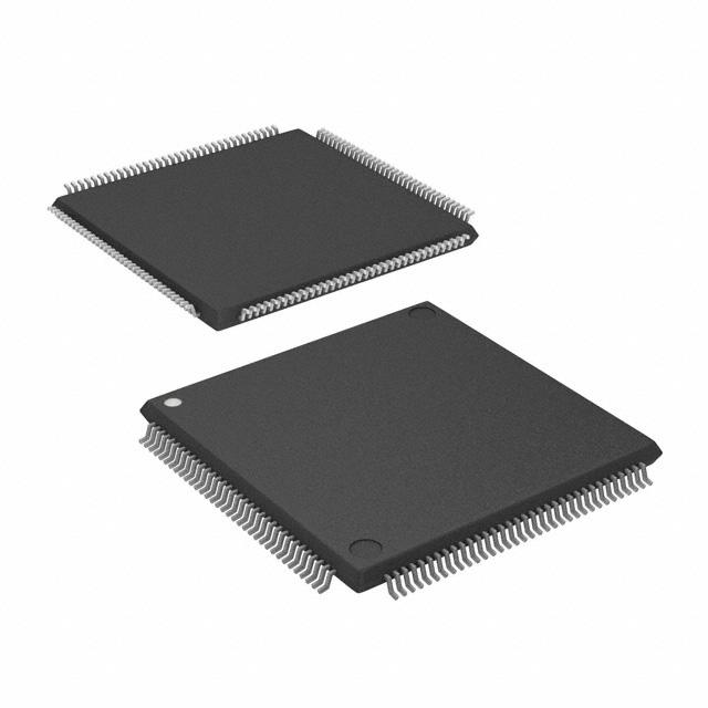
A54SX16A-2TQG144I ECAD Model
A54SX16A-2TQG144I Attributes
| Type | Description | Select |
|---|---|---|
| Rohs Code | Yes | |
| Part Life Cycle Code | Transferred | |
| Supply Voltage-Nom | 2.5 V | |
| Number of Inputs | 113 | |
| Number of Outputs | 113 | |
| Number of Logic Cells | 1452 | |
| Number of Equivalent Gates | 24000 | |
| Number of CLBs | 1452 | |
| Combinatorial Delay of a CLB-Max | 1 ns | |
| Programmable Logic Type | FIELD PROGRAMMABLE GATE ARRAY | |
| Temperature Grade | INDUSTRIAL | |
| Package Shape | SQUARE | |
| Technology | CMOS | |
| Organization | 1452 CLBS, 24000 GATES | |
| Additional Feature | 16000 TYPICAL GATES AVAILABLE | |
| Clock Frequency-Max | 294 MHz | |
| Power Supplies | 2.5,3.3/5 V | |
| Supply Voltage-Max | 2.75 V | |
| Supply Voltage-Min | 2.25 V | |
| JESD-30 Code | S-PQFP-G144 | |
| Qualification Status | Not Qualified | |
| JESD-609 Code | e3 | |
| Moisture Sensitivity Level | 3 | |
| Operating Temperature-Max | 85 °C | |
| Operating Temperature-Min | -40 °C | |
| Number of Terminals | 144 | |
| Package Body Material | PLASTIC/EPOXY | |
| Package Code | LFQFP | |
| Package Equivalence Code | QFP144,.87SQ,20 | |
| Package Shape | SQUARE | |
| Package Style | FLATPACK, LOW PROFILE, FINE PITCH | |
| Surface Mount | YES | |
| Terminal Finish | MATTE TIN | |
| Terminal Form | GULL WING | |
| Terminal Pitch | 500 µm | |
| Terminal Position | QUAD | |
| Width | 20 mm | |
| Length | 20 mm | |
| Seated Height-Max | 1.6 mm | |
| Ihs Manufacturer | MICROSEMI CORP | |
| Package Description | LFQFP, QFP144,.87SQ,20 | |
| Reach Compliance Code | compliant | |
| HTS Code | 8542.39.00.01 |
A54SX16A-2TQG144I Datasheet Download
A54SX16A-2TQG144I Overview
The A54SX16A-2TQG144I is an FPGA chip model from Xilinx, a leading manufacturer of programmable logic devices. It is a member of the Virtex-5 family of FPGAs, which are designed for high-performance applications. The chip features 16 million system gates, two independent power planes, and a wide range of I/O options. It is designed for use in high-speed communications, high-performance computing, and embedded applications.
The A54SX16A-2TQG144I has a wide range of features that enable it to be used in a variety of applications. It has 16 million system gates, which are divided into two independent power planes for improved power efficiency. It also has two independent clock networks, which provide the flexibility to support high-speed data transfer and synchronization. Additionally, the chip has up to 144 I/O pins, with up to 12 high-speed differential I/O pairs. It also supports a wide range of I/O standards, including LVDS, LVPECL, and SSTL.
The A54SX16A-2TQG144I can be used in a variety of applications, including high-speed communications, high-performance computing, and embedded systems. In communications applications, the chip can be used to provide high-speed data transfer and synchronization. In high-performance computing applications, the chip can be used to provide high-speed data processing, as well as to provide a platform for complex algorithms. Finally, in embedded applications, the chip can be used to provide a platform for embedded systems, such as digital signal processors, microcontrollers, and other embedded devices.
Overall, the A54SX16A-2TQG144I is a powerful FPGA chip model from Xilinx, designed for use in high-speed communications, high-performance computing, and embedded applications. It features 16 million system gates, two independent power planes, and a wide range of I/O options. It is a reliable and powerful chip, capable of providing the performance and flexibility needed for a variety of applications.
You May Also Be Interested In

1,571 In Stock
Pricing (USD)
| QTY | Unit Price | Ext Price |
|---|---|---|
| 1+ | $132.7259 | $132.7259 |
| 10+ | $131.2987 | $1,312.9872 |
| 100+ | $124.1629 | $12,416.2920 |
| 1000+ | $117.0271 | $58,513.5600 |
| 10000+ | $107.0370 | $107,037.0000 |
| The price is for reference only, please refer to the actual quotation! | ||