
Microchip Technology Inc
A54SX16A-2TQG144
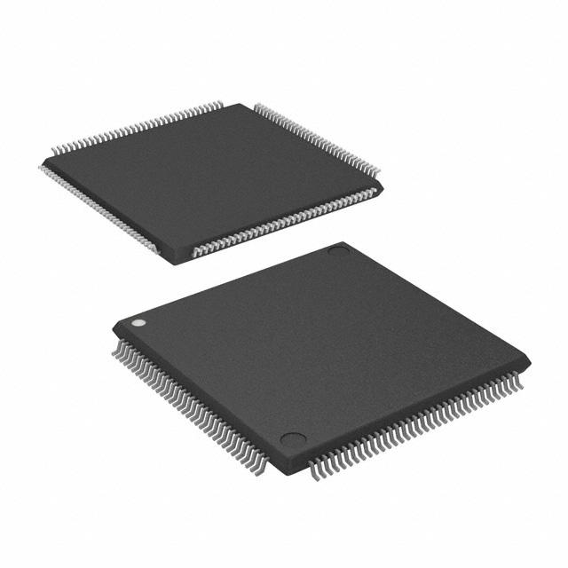
A54SX16A-2TQG144 ECAD Model
A54SX16A-2TQG144 Attributes
| Type | Description | Select |
|---|---|---|
| Rohs Code | Yes | |
| Part Life Cycle Code | Transferred | |
| Supply Voltage-Nom | 2.5 V | |
| Number of Inputs | 113 | |
| Number of Outputs | 113 | |
| Number of Logic Cells | 1452 | |
| Number of Equivalent Gates | 24000 | |
| Number of CLBs | 1452 | |
| Combinatorial Delay of a CLB-Max | 1 ns | |
| Programmable Logic Type | FIELD PROGRAMMABLE GATE ARRAY | |
| Temperature Grade | COMMERCIAL | |
| Package Shape | SQUARE | |
| Technology | CMOS | |
| Organization | 1452 CLBS, 24000 GATES | |
| Additional Feature | 16000 TYPICAL GATES AVAILABLE | |
| Clock Frequency-Max | 294 MHz | |
| Power Supplies | 2.5,3.3/5 V | |
| Supply Voltage-Max | 2.75 V | |
| Supply Voltage-Min | 2.25 V | |
| JESD-30 Code | S-PQFP-G144 | |
| Qualification Status | Not Qualified | |
| JESD-609 Code | e3 | |
| Moisture Sensitivity Level | 3 | |
| Operating Temperature-Max | 70 °C | |
| Number of Terminals | 144 | |
| Package Body Material | PLASTIC/EPOXY | |
| Package Code | LFQFP | |
| Package Equivalence Code | QFP144,.87SQ,20 | |
| Package Shape | SQUARE | |
| Package Style | FLATPACK, LOW PROFILE, FINE PITCH | |
| Surface Mount | YES | |
| Terminal Finish | MATTE TIN | |
| Terminal Form | GULL WING | |
| Terminal Pitch | 500 µm | |
| Terminal Position | QUAD | |
| Width | 20 mm | |
| Length | 20 mm | |
| Seated Height-Max | 1.6 mm | |
| Ihs Manufacturer | MICROSEMI CORP | |
| Package Description | LFQFP, QFP144,.87SQ,20 | |
| Reach Compliance Code | compliant | |
| HTS Code | 8542.39.00.01 |
A54SX16A-2TQG144 Datasheet Download
A54SX16A-2TQG144 Overview
The A54SX16A-2TQG144 is a high-performance, low-power, low-cost FPGA chip model designed by Xilinx. It is a member of the Spartan-6 family of FPGAs, and is based on the latest 45nm technology. The chip is a 16-bit, 2-input multiplexer (MUX) with an integrated 144-bit wide memory interface. It has a total of 17,280 logic cells, and is capable of supporting up to 18,432 user I/O pins. It also has a total of 72 18Kb block RAMs, and four DSP slices.
The A54SX16A-2TQG144 has a maximum clock frequency of 250MHz and a power dissipation of 1.2W. It has a total of 5,400 flip-flops and 5,400 latches, and is capable of handling up to 4,500 user-defined functions. The chip also has advanced features such as clock gating, power-down modes, and programmable output delay.
The A54SX16A-2TQG144 is ideal for use in a variety of applications, such as high-speed data processing, high-speed networking, video and image processing, and embedded systems. It is also suitable for use in industrial, automotive, and military applications. The chip is designed to be used in conjunction with Xilinx's ISE Design Suite, which provides a comprehensive set of tools for designing and debugging FPGA designs.
You May Also Be Interested In

5,153 In Stock
Pricing (USD)
| QTY | Unit Price | Ext Price |
|---|---|---|
| 1+ | $113.8766 | $113.8766 |
| 10+ | $112.6522 | $1,126.5216 |
| 100+ | $106.5298 | $10,652.9760 |
| 1000+ | $100.4074 | $50,203.6800 |
| 10000+ | $91.8360 | $91,836.0000 |
| The price is for reference only, please refer to the actual quotation! | ||