
Microchip Technology Inc
A40MX02-PLG44I
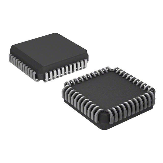
A40MX02-PLG44I ECAD Model
A40MX02-PLG44I Attributes
| Type | Description | Select |
|---|---|---|
| Rohs Code | Yes | |
| Part Life Cycle Code | Transferred | |
| Supply Voltage-Nom | 3.3 V | |
| Number of Equivalent Gates | 3000 | |
| Number of CLBs | 295 | |
| Combinatorial Delay of a CLB-Max | 2.7 ns | |
| Programmable Logic Type | FIELD PROGRAMMABLE GATE ARRAY | |
| Temperature Grade | INDUSTRIAL | |
| Package Shape | SQUARE | |
| Technology | CMOS | |
| Organization | 295 CLBS, 3000 GATES | |
| Additional Feature | ALSO OPERATES AT 5V SUPPLY | |
| Clock Frequency-Max | 80 MHz | |
| Supply Voltage-Max | 3.6 V | |
| Supply Voltage-Min | 3 V | |
| JESD-30 Code | S-PQCC-J44 | |
| Qualification Status | Not Qualified | |
| JESD-609 Code | e3 | |
| Moisture Sensitivity Level | 3 | |
| Operating Temperature-Max | 85 °C | |
| Operating Temperature-Min | -40 °C | |
| Number of Terminals | 44 | |
| Package Body Material | PLASTIC/EPOXY | |
| Package Code | QCCJ | |
| Package Shape | SQUARE | |
| Package Style | CHIP CARRIER | |
| Surface Mount | YES | |
| Terminal Finish | TIN | |
| Terminal Form | J BEND | |
| Terminal Pitch | 1.27 mm | |
| Terminal Position | QUAD | |
| Width | 16.5862 mm | |
| Length | 16.5862 mm | |
| Seated Height-Max | 4.572 mm | |
| Ihs Manufacturer | MICROSEMI CORP | |
| Package Description | QCCJ, | |
| Reach Compliance Code | compliant | |
| HTS Code | 8542.39.00.01 |
A40MX02-PLG44I Datasheet Download
A40MX02-PLG44I Overview
The A40MX02-PLG44I is a Field Programmable Gate Array (FPGA) chip model created by Altera Corporation. It is a low-cost, low-power device that is suitable for a variety of applications. The device features a 4K-bit embedded RAM, a 32-bit RISC processor, and a variety of digital signal processing (DSP) blocks.
The device has a total of 44 I/O pins, with 2 of them being dedicated to a JTAG port. It has a total of 4-bit wide memory ports and a total of 4-bit wide I/O ports. It also has a total of 4-bit wide logic blocks. The device supports a variety of programming languages, including Verilog, VHDL, and C. It also supports a variety of development tools, such as Quartus II, Nios II, and ModelSim.
The A40MX02-PLG44I is suitable for a variety of applications, including communications, consumer electronics, automotive, and industrial control. It can be used to create a variety of digital systems, such as logic controllers, data acquisition systems, and digital signal processing systems. It is also suitable for applications that require low-power, low-cost solutions.
In summary, the A40MX02-PLG44I is a low-cost and low-power FPGA chip model that is suitable for a variety of applications. It features a 4K-bit embedded RAM, a 32-bit RISC processor, and a variety of digital signal processing blocks. It has a total of 44 I/O pins, with 2 of them being dedicated to a JTAG port. It supports a variety of programming languages and development tools and is suitable for a variety of applications.
You May Also Be Interested In

1,479 In Stock
Pricing (USD)
| QTY | Unit Price | Ext Price |
|---|---|---|
| 1+ | $59.8289 | $59.8289 |
| 10+ | $59.1856 | $591.8562 |
| 100+ | $55.9690 | $5,596.9014 |
| 1000+ | $52.7524 | $26,376.2020 |
| 10000+ | $48.2492 | $48,249.1500 |
| The price is for reference only, please refer to the actual quotation! | ||