
Microchip Technology Inc
A40MX02-3PL68I
A40MX02-3PL68I ECAD Model
A40MX02-3PL68I Attributes
| Type | Description | Select |
|---|---|---|
| Mfr | Microchip Technology | |
| Series | MX | |
| Package | Tray | |
| Number of I/O | 57 | |
| Number of Gates | 3000 | |
| Voltage - Supply | 3V ~ 3.6V, 4.5V ~ 5.5V | |
| Mounting Type | Surface Mount | |
| Operating Temperature | -40°C ~ 85°C (TA) | |
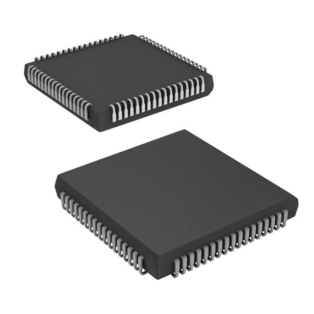
| Package / Case | 68-LCC (J-Lead) | |
| Supplier Device Package | 68-PLCC (24.23x24.23) | |
| Base Product Number | A40MX02 |
A40MX02-3PL68I Datasheet Download
A40MX02-3PL68I Overview
The A40MX02-3PL68I chip is a high-speed, low-power, field-programmable gate array (FPGA) device from Lattice Semiconductor. It is based on the MachXO2 family of FPGAs, which are designed to provide a cost-effective and reliable solution for a wide range of embedded control and interface applications.
The A40MX02-3PL68I chip has a total of 4,096 logic cells and 4,096 flip-flops, and offers a maximum clock frequency of up to 300 MHz. It supports up to 16 I/O banks and up to 256 user I/O pins. It also includes up to 4Kbits of SRAM, up to 256Kbits of flash memory, and up to 8Kbits of EEPROM memory.
The A40MX02-3PL68I chip is suitable for use in a variety of applications, such as industrial automation, consumer electronics, automotive, and medical. It is also suitable for applications such as motor control, power management, communication, and signal processing.
The A40MX02-3PL68I chip is available in a 68-pin VQFN package, and is RoHS compliant. It is also supported by the MachXO2 development environment, which provides a comprehensive set of tools and libraries for designing and debugging applications.
You May Also Be Interested In
5,731 In Stock
Pricing (USD)
| QTY | Unit Price | Ext Price |
|---|---|---|
| No reference price found. | ||