
Microchip Technology Inc
A40MX02-2PLG68I
A40MX02-2PLG68I ECAD Model
A40MX02-2PLG68I Attributes
| Type | Description | Select |
|---|---|---|
| Rohs Code | Yes | |
| Part Life Cycle Code | Transferred | |
| Supply Voltage-Nom | 3.3 V | |
| Number of Equivalent Gates | 3000 | |
| Number of CLBs | 295 | |
| Combinatorial Delay of a CLB-Max | 2 ns | |
| Programmable Logic Type | FIELD PROGRAMMABLE GATE ARRAY | |
| Temperature Grade | INDUSTRIAL | |
| Package Shape | SQUARE | |
| Technology | CMOS | |
| Organization | 295 CLBS, 3000 GATES | |
| Additional Feature | ALSO OPERATES AT 5V SUPPLY | |
| Clock Frequency-Max | 101 MHz | |
| Supply Voltage-Max | 3.6 V | |
| Supply Voltage-Min | 3 V | |
| JESD-30 Code | S-PQCC-J68 | |
| Qualification Status | Not Qualified | |
| JESD-609 Code | e3 | |
| Moisture Sensitivity Level | 3 | |
| Operating Temperature-Max | 85 °C | |
| Operating Temperature-Min | -40 °C | |
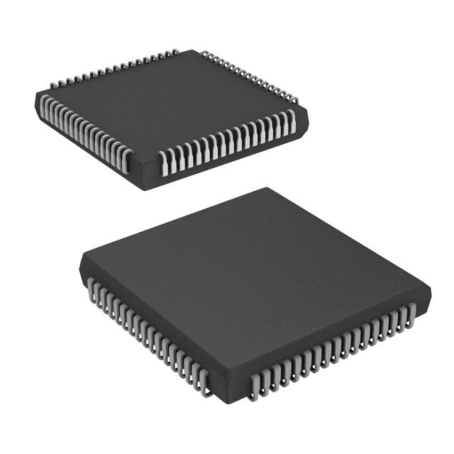
| Number of Terminals | 68 | |
| Package Body Material | PLASTIC/EPOXY | |
| Package Code | QCCJ | |
| Package Shape | SQUARE | |
| Package Style | CHIP CARRIER | |
| Surface Mount | YES | |
| Terminal Finish | MATTE TIN | |
| Terminal Form | J BEND | |
| Terminal Pitch | 1.27 mm | |
| Terminal Position | QUAD | |
| Width | 24.2316 mm | |
| Length | 24.2316 mm | |
| Seated Height-Max | 4.572 mm | |
| Ihs Manufacturer | MICROSEMI CORP | |
| Package Description | QCCJ, | |
| Reach Compliance Code | compliant | |
| HTS Code | 8542.39.00.01 |
A40MX02-2PLG68I Datasheet Download
A40MX02-2PLG68I Overview
The A40MX02-2PLG68I is a Field Programmable Gate Array (FPGA) chip, manufactured by Actel Corporation. It is a low-cost, low-power device based on the company’s proprietary ProASIC3 architecture. This chip is designed to provide a high level of integration, flexibility and scalability for a variety of applications.
The A40MX02-2PLG68I has a total of 68 I/O pins, and is available in a standard PLCC68 package. It also features an integrated Flash memory, which can be used to store program data and configuration information. The device has a maximum operating frequency of 200 MHz, and a total power consumption of 1.2 W. It also has an integrated phase-locked loop (PLL), which can be used to generate high-speed clock signals.
The A40MX02-2PLG68I is suitable for a wide range of applications, including industrial automation, consumer electronics, automotive, medical, and aerospace. It can be used to implement complex logic designs, and is also suitable for high-speed logic designs. It is also capable of supporting multiple protocols, such as Ethernet and USB.
In summary, the A40MX02-2PLG68I is a low-cost, low-power FPGA device, with a high level of integration and flexibility. It is suitable for a variety of applications, and can be used to implement complex logic designs. It also has an integrated Flash memory and PLL, which can be used to generate high-speed clock signals.
You May Also Be Interested In

2,184 In Stock
Pricing (USD)
| QTY | Unit Price | Ext Price |
|---|---|---|
| 1+ | $77.3946 | $77.3946 |
| 10+ | $76.5624 | $765.6240 |
| 100+ | $72.4014 | $7,240.1400 |
| 1000+ | $68.2404 | $34,120.2000 |
| 10000+ | $62.4150 | $62,415.0000 |
| The price is for reference only, please refer to the actual quotation! | ||