
Microchip Technology Inc
A40MX02-1PLG68M
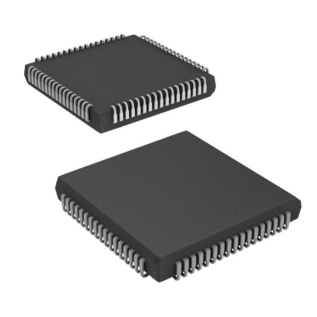
A40MX02-1PLG68M ECAD Model
A40MX02-1PLG68M Attributes
| Type | Description | Select |
|---|---|---|
| Rohs Code | Yes | |
| Part Life Cycle Code | Transferred | |
| Supply Voltage-Nom | 3.3 V | |
| Number of Equivalent Gates | 3000 | |
| Number of CLBs | 295 | |
| Combinatorial Delay of a CLB-Max | 2.3 ns | |
| Programmable Logic Type | FIELD PROGRAMMABLE GATE ARRAY | |
| Temperature Grade | MILITARY | |
| Package Shape | SQUARE | |
| Technology | CMOS | |
| Organization | 295 CLBS, 3000 GATES | |
| Additional Feature | ALSO OPERATES AT 5V SUPPLY | |
| Clock Frequency-Max | 92 MHz | |
| Supply Voltage-Max | 3.6 V | |
| Supply Voltage-Min | 3 V | |
| JESD-30 Code | S-PQCC-J68 | |
| Qualification Status | Not Qualified | |
| JESD-609 Code | e3 | |
| Moisture Sensitivity Level | 3 | |
| Operating Temperature-Max | 125 °C | |
| Operating Temperature-Min | -55 °C | |
| Number of Terminals | 68 | |
| Package Body Material | PLASTIC/EPOXY | |
| Package Code | QCCJ | |
| Package Shape | SQUARE | |
| Package Style | CHIP CARRIER | |
| Surface Mount | YES | |
| Terminal Finish | MATTE TIN | |
| Terminal Form | J BEND | |
| Terminal Pitch | 1.27 mm | |
| Terminal Position | QUAD | |
| Width | 24.2316 mm | |
| Length | 24.2316 mm | |
| Seated Height-Max | 4.572 mm | |
| Ihs Manufacturer | MICROSEMI CORP | |
| Package Description | QCCJ, | |
| Reach Compliance Code | compliant | |
| HTS Code | 8542.39.00.01 | |
| ECCN Code | 3A001.A.2.C |
A40MX02-1PLG68M Datasheet Download
A40MX02-1PLG68M Overview
The A40MX02-1PLG68M is a low-power, low-cost, high-performance, Field Programmable Gate Array (FPGA) chip from the Altera Cyclone IV family. It has a maximum of 4,096 logic elements and 4,096 embedded memory blocks. The chip also has 132 user I/O pins, two phase-locked loop (PLL) clock management units, and two high-speed transceivers.
The A40MX02-1PLG68M is a cost-efficient FPGA solution for a wide range of applications, offering high performance and low power consumption. It is suitable for applications such as automotive, industrial, consumer, medical, and aerospace. It is also suitable for applications such as image processing, signal processing, and communication systems.
The chip has a maximum power dissipation of 3.5 W, a maximum operating frequency of 150 MHz, and a minimum operating voltage of 1.2 V. It is also capable of operating at temperatures ranging from -40°C to 85°C. The chip has a built-in static power reduction feature which helps to reduce power consumption during idle periods.
The A40MX02-1PLG68M chip is also equipped with an on-chip debug feature which allows for debugging of the FPGA design. The chip also supports in-system programmability (ISP) which allows for the reprogramming of the FPGA without the need for external programming tools.
In conclusion, the A40MX02-1PLG68M is a low-power, high-performance, cost-effective FPGA chip with a wide range of applications. It is suitable for automotive, industrial, consumer, medical, and aerospace applications, as well as image processing, signal processing, and communication systems. It is also equipped with an on-chip debug feature and supports in-system programmability.
You May Also Be Interested In

5,145 In Stock
Pricing (USD)
| QTY | Unit Price | Ext Price |
|---|---|---|
| 1+ | $334.6144 | $334.6144 |
| 10+ | $331.0164 | $3,310.1637 |
| 100+ | $313.0263 | $31,302.6348 |
| 1000+ | $295.0363 | $147,518.1640 |
| 10000+ | $269.8503 | $269,850.3000 |
| The price is for reference only, please refer to the actual quotation! | ||