
Microchip Technology Inc
A3PN125-VQ100
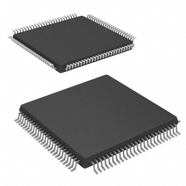
A3PN125-VQ100 ECAD Model
A3PN125-VQ100 Attributes
| Type | Description | Select |
|---|---|---|
| Rohs Code | No | |
| Part Life Cycle Code | Transferred | |
| Supply Voltage-Nom | 1.5 V | |
| Number of Equivalent Gates | 125000 | |
| Number of CLBs | 3072 | |
| Programmable Logic Type | FIELD PROGRAMMABLE GATE ARRAY | |
| Temperature Grade | OTHER | |
| Package Shape | SQUARE | |
| Technology | CMOS | |
| Organization | 3072 CLBS, 125000 GATES | |
| Supply Voltage-Max | 1.575 V | |
| Supply Voltage-Min | 1.425 V | |
| JESD-30 Code | S-PQFP-G100 | |
| Qualification Status | Not Qualified | |
| JESD-609 Code | e0 | |
| Moisture Sensitivity Level | 3 | |
| Operating Temperature-Max | 70 °C | |
| Operating Temperature-Min | -20 °C | |
| Number of Terminals | 100 | |
| Package Body Material | PLASTIC/EPOXY | |
| Package Code | TFQFP | |
| Package Shape | SQUARE | |
| Package Style | FLATPACK, THIN PROFILE, FINE PITCH | |
| Surface Mount | YES | |
| Terminal Finish | TIN LEAD | |
| Terminal Form | GULL WING | |
| Terminal Pitch | 500 µm | |
| Terminal Position | QUAD | |
| Width | 14 mm | |
| Length | 14 mm | |
| Seated Height-Max | 1.2 mm | |
| Ihs Manufacturer | MICROSEMI CORP | |
| Package Description | TFQFP, | |
| Reach Compliance Code | unknown | |
| HTS Code | 8542.39.00.01 |
A3PN125-VQ100 Datasheet Download
A3PN125-VQ100 Overview
The A3PN125-VQ100 is a chip model designed by Altera Corporation. It is a field-programmable gate array (FPGA) chip that is used in a wide range of applications. The chip has a maximum operating frequency of 125 MHz and contains over 1 million logic elements. It is fabricated using a 0.18-micron CMOS process and contains up to 125Kbits of embedded memory. It also supports up to 8 banks of embedded SRAM.
The A3PN125-VQ100 chip is designed for a variety of applications, including embedded systems, industrial automation, medical electronics, consumer electronics, and automotive systems. It is also suitable for applications such as digital signal processing, image processing, and communication systems.
The A3PN125-VQ100 chip is equipped with a wide range of features and functions. It has a total of 8 I/O banks, each with up to 5V support, and can support up to 200 I/O pins. It also supports up to 8 banks of embedded SRAM, and can be configured to support up to 128Kbits of embedded memory. Additionally, it has an on-chip JTAG controller and a wide range of I/O features, such as LVTTL, LVCMOS, and PCI.
The A3PN125-VQ100 chip is designed to be used in a wide range of applications. It is suitable for use in embedded systems, industrial automation, medical electronics, consumer electronics, and automotive systems. It is also suitable for applications such as digital signal processing, image processing, and communication systems. Additionally, it can be used for a variety of other applications, such as high-speed logic design and prototyping.
You May Also Be Interested In

3,639 In Stock
Pricing (USD)
| QTY | Unit Price | Ext Price |
|---|---|---|
| 1+ | $9.9764 | $9.9764 |
| 10+ | $9.8691 | $98.6912 |
| 100+ | $9.3328 | $933.2751 |
| 1000+ | $8.7964 | $4,398.1930 |
| 10000+ | $8.0455 | $8,045.4750 |
| The price is for reference only, please refer to the actual quotation! | ||