
Microchip Technology Inc
A3PN010-2QNG48I
A3PN010-2QNG48I ECAD Model
A3PN010-2QNG48I Attributes
| Type | Description | Select |
|---|---|---|
| Rohs Code | Yes | |
| Part Life Cycle Code | Transferred | |
| Supply Voltage-Nom | 1.5 V | |
| Number of Equivalent Gates | 10000 | |
| Number of CLBs | 260 | |
| Programmable Logic Type | FIELD PROGRAMMABLE GATE ARRAY | |
| Temperature Grade | INDUSTRIAL | |
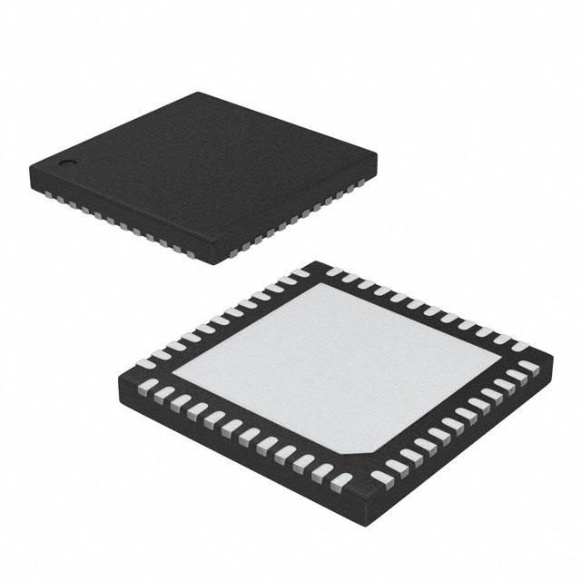
| Package Shape | SQUARE | |
| Technology | CMOS | |
| Organization | 260 CLBS, 10000 GATES | |
| Supply Voltage-Max | 1.575 V | |
| Supply Voltage-Min | 1.425 V | |
| JESD-30 Code | S-XQCC-N48 | |
| Qualification Status | Not Qualified | |
| Moisture Sensitivity Level | 3 | |
| Operating Temperature-Max | 85 °C | |
| Operating Temperature-Min | -40 °C | |
| Number of Terminals | 48 | |
| Package Body Material | UNSPECIFIED | |
| Package Code | HQCCN | |
| Package Shape | SQUARE | |
| Package Style | CHIP CARRIER, HEAT SINK/SLUG | |
| Surface Mount | YES | |
| Terminal Form | NO LEAD | |
| Terminal Pitch | 400 µm | |
| Terminal Position | QUAD | |
| Width | 6 mm | |
| Length | 6 mm | |
| Ihs Manufacturer | MICROSEMI CORP | |
| Package Description | HQCCN, | |
| Reach Compliance Code | compliant | |
| HTS Code | 8542.39.00.01 |
A3PN010-2QNG48I Datasheet Download
A3PN010-2QNG48I Overview
The A3PN010-2QNG48I is a low power, low voltage, high performance, field programmable gate array (FPGA) chip from the Altera Corporation. It is based on the Stratix III architecture and is designed for high-end applications such as embedded systems, communications, military, aerospace, and medical.
The A3PN010-2QNG48I FPGA chip has a total of 1,024 logic elements and 4,096 bits of RAM. It also has four dedicated clock management tiles, 10 high-speed SERDES transceivers, and 4,096 bits of distributed RAM. The FPGA chip also has a total of 48 I/O pins, which can be configured as either single-ended or differential pairs. The chip operates at a voltage of 1.2V and has a maximum power consumption of 4.4W.
The A3PN010-2QNG48I is designed to provide high-speed and low-power performance. It has a maximum clock frequency of 250MHz and a maximum operating temperature of 85°C. It also has a built-in thermal management system to ensure the chip remains within its specified operating temperature range.
The A3PN010-2QNG48I FPGA chip is suitable for a wide range of applications. It can be used in high-speed data acquisition, digital signal processing, communications, embedded systems, medical, military, and aerospace applications. The chip also supports various development tools, including the Quartus II design software and the Nios II embedded development suite.
You May Also Be Interested In

5,861 In Stock
Pricing (USD)
| QTY | Unit Price | Ext Price |
|---|---|---|
| No reference price found. | ||