
Microchip Technology Inc
A3PE600-FGG484I
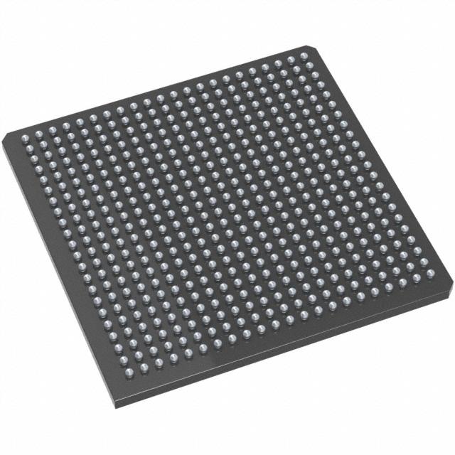
A3PE600-FGG484I ECAD Model
A3PE600-FGG484I Attributes
| Type | Description | Select |
|---|---|---|
| Rohs Code | Yes | |
| Part Life Cycle Code | Transferred | |
| Supply Voltage-Nom | 1.5 V | |
| Number of Inputs | 270 | |
| Number of Outputs | 270 | |
| Number of Logic Cells | 13824 | |
| Number of Equivalent Gates | 600000 | |
| Number of CLBs | 13824 | |
| Programmable Logic Type | FIELD PROGRAMMABLE GATE ARRAY | |
| Temperature Grade | INDUSTRIAL | |
| Package Shape | SQUARE | |
| Technology | CMOS | |
| Organization | 13824 CLBS, 600000 GATES | |
| Clock Frequency-Max | 350 MHz | |
| Power Supplies | 1.5/3.3 V | |
| Supply Voltage-Max | 1.575 V | |
| Supply Voltage-Min | 1.425 V | |
| JESD-30 Code | S-PBGA-B484 | |
| Qualification Status | Not Qualified | |
| JESD-609 Code | e1 | |
| Moisture Sensitivity Level | 3 | |
| Operating Temperature-Max | 85 °C | |
| Operating Temperature-Min | -40 °C | |
| Peak Reflow Temperature (Cel) | 250 | |
| Time@Peak Reflow Temperature-Max (s) | 30 | |
| Number of Terminals | 484 | |
| Package Body Material | PLASTIC/EPOXY | |
| Package Code | BGA | |
| Package Equivalence Code | BGA484,22X22,40 | |
| Package Shape | SQUARE | |
| Package Style | GRID ARRAY | |
| Surface Mount | YES | |
| Terminal Finish | TIN SILVER COPPER | |
| Terminal Form | BALL | |
| Terminal Pitch | 1 mm | |
| Terminal Position | BOTTOM | |
| Width | 23 mm | |
| Length | 23 mm | |
| Seated Height-Max | 2.44 mm | |
| Ihs Manufacturer | MICROSEMI CORP | |
| Package Description | BGA, BGA484,22X22,40 | |
| Reach Compliance Code | compliant | |
| HTS Code | 8542.39.00.01 |
A3PE600-FGG484I Datasheet Download
A3PE600-FGG484I Overview
The A3PE600-FGG484I chip model is a programmable logic device from Altera, the world’s leading provider of FPGAs, CPLDs and other programmable logic solutions. It is a high-performance, low-power, and cost-effective solution for a variety of applications.
The A3PE600-FGG484I chip model is based on the Stratix III architecture, and offers a range of features and benefits. It has a total of 484,000 logic elements, and a total of 6,000 embedded memory blocks. It also features up to 1,024 18x18 multipliers, and up to 8,192 I/O pins. The device is capable of operating at speeds up to 500MHz, and can be used with a variety of I/O standards, including LVDS, LVPECL, and HSTL.
The A3PE600-FGG484I chip model is ideal for a variety of applications, including communications, networking, industrial automation, medical imaging, and video processing. It is also well-suited for applications that require high-speed, low-power, and cost-effective solutions. Additionally, the device is compatible with Altera’s Quartus II software, which makes it easy to configure the device for a variety of applications.
Overall, the A3PE600-FGG484I chip model is a powerful and cost-effective solution for a variety of applications. It offers a range of features and benefits, including high performance, low power consumption, and compatibility with Altera’s Quartus II software. As such, it is an ideal choice for a variety of applications, including communications, networking, industrial automation, medical imaging, and video processing.
You May Also Be Interested In

2,205 In Stock
Pricing (USD)
| QTY | Unit Price | Ext Price |
|---|---|---|
| 1+ | $78.8645 | $78.8645 |
| 10+ | $78.0165 | $780.1646 |
| 100+ | $73.7764 | $7,377.6435 |
| 1000+ | $69.5364 | $34,768.2050 |
| 10000+ | $63.6004 | $63,600.3750 |
| The price is for reference only, please refer to the actual quotation! | ||