

Microchip Technology Inc
A3PE1500-FG676
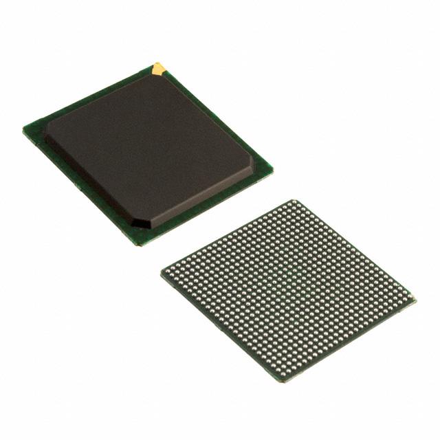
A3PE1500-FG676 ECAD Model
A3PE1500-FG676 Attributes
| Type | Description | Select |
|---|---|---|
| Rohs Code | No | |
| Part Life Cycle Code | Transferred | |
| Supply Voltage-Nom | 1.5 V | |
| Number of Inputs | 444 | |
| Number of Outputs | 444 | |
| Number of Logic Cells | 38400 | |
| Number of Equivalent Gates | 1500000 | |
| Number of CLBs | 38400 | |
| Programmable Logic Type | FIELD PROGRAMMABLE GATE ARRAY | |
| Temperature Grade | COMMERCIAL | |
| Package Shape | SQUARE | |
| Technology | CMOS | |
| Organization | 38400 CLBS, 1500000 GATES | |
| Clock Frequency-Max | 350 MHz | |
| Power Supplies | 1.5/3.3 V | |
| Supply Voltage-Max | 1.575 V | |
| Supply Voltage-Min | 1.425 V | |
| JESD-30 Code | S-PBGA-B676 | |
| Qualification Status | Not Qualified | |
| JESD-609 Code | e0 | |
| Moisture Sensitivity Level | 3 | |
| Operating Temperature-Max | 70 °C | |
| Number of Terminals | 676 | |
| Package Body Material | PLASTIC/EPOXY | |
| Package Code | BGA | |
| Package Equivalence Code | BGA676,26X26,40 | |
| Package Shape | SQUARE | |
| Package Style | GRID ARRAY | |
| Surface Mount | YES | |
| Terminal Finish | TIN LEAD | |
| Terminal Form | BALL | |
| Terminal Pitch | 1 mm | |
| Terminal Position | BOTTOM | |
| Width | 27 mm | |
| Length | 27 mm | |
| Seated Height-Max | 2.44 mm | |
| Ihs Manufacturer | MICROSEMI CORP | |
| Package Description | BGA, BGA676,26X26,40 | |
| Reach Compliance Code | unknown | |
| HTS Code | 8542.39.00.01 |
A3PE1500-FG676 Datasheet Download
A3PE1500-FG676 Overview
The A3PE1500-FG676 is a high-performance FPGA (Field Programmable Gate Array) chip designed and manufactured by Altera. It is a member of the Cyclone III FPGA family and provides a high level of integration and performance.
The chip has a total of 676 logic elements, each of which can be configured to perform a variety of logic functions. It also has 8Kbits of embedded memory, 18 multipliers, and a total of 4 DSP blocks. It has a total of 4 I/O banks, each of which can support up to 72 I/O pins. The I/O pins are configurable as either LVTTL or LVCMOS. The chip has a total of 10 dedicated clock pins, which can be used to generate and manage high-speed clock signals.
The A3PE1500-FG676 is suitable for a wide range of applications, including digital signal processing, video processing, networking, and embedded systems. It is also suitable for use in high-speed data acquisition systems and for implementing complex control algorithms.
The chip is available in a range of packages, including a 208-pin PQFP and a 256-pin BGA. It has a maximum operating temperature of 85°C and an operating voltage range of 1.2V to 3.3V. It is also RoHS compliant and is available in both industrial and commercial temperature grades.
You May Also Be Interested In

4,669 In Stock
Pricing (USD)
| QTY | Unit Price | Ext Price |
|---|---|---|
| 1+ | $179.8892 | $179.8892 |
| 10+ | $177.9549 | $1,779.5486 |
| 100+ | $168.2834 | $16,828.3404 |
| 1000+ | $158.6119 | $79,305.9720 |
| 10000+ | $145.0719 | $145,071.9000 |
| The price is for reference only, please refer to the actual quotation! | ||