
Microchip Technology Inc
A3P600-FG484I
A3P600-FG484I ECAD Model
A3P600-FG484I Attributes
| Type | Description | Select |
|---|---|---|
| Rohs Code | No | |
| Part Life Cycle Code | Transferred | |
| Supply Voltage-Nom | 1.5 V | |
| Number of Equivalent Gates | 600000 | |
| Programmable Logic Type | FIELD PROGRAMMABLE GATE ARRAY | |
| Temperature Grade | INDUSTRIAL | |
| Package Shape | SQUARE | |
| Technology | CMOS | |
| Organization | 600000 GATES | |
| Supply Voltage-Max | 1.575 V | |
| Supply Voltage-Min | 1.425 V | |
| JESD-30 Code | S-PBGA-B484 | |
| Qualification Status | Not Qualified | |
| Operating Temperature-Max | 85 °C | |
| Operating Temperature-Min | -40 °C | |
| Peak Reflow Temperature (Cel) | NOT SPECIFIED | |
| Time@Peak Reflow Temperature-Max (s) | NOT SPECIFIED | |
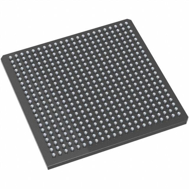
| Number of Terminals | 484 | |
| Package Body Material | PLASTIC/EPOXY | |
| Package Code | BGA | |
| Package Shape | SQUARE | |
| Package Style | GRID ARRAY | |
| Surface Mount | YES | |
| Terminal Form | BALL | |
| Terminal Pitch | 1 mm | |
| Terminal Position | BOTTOM | |
| Width | 27 mm | |
| Length | 27 mm | |
| Seated Height-Max | 2.44 mm | |
| Ihs Manufacturer | ACTEL CORP | |
| Reach Compliance Code | unknown | |
| Package Description | 1 MM PITCH, FBGA-484 |
A3P600-FG484I Datasheet Download
A3P600-FG484I Overview
The A3P600-FG484I is a FPGA (Field Programmable Gate Array) chip model manufactured by Altera. It is a high-performance, low-cost FPGA with very low power consumption. It has a total of 484 logic elements and 4,608 logic registers. The logic elements are organized into 16 logic blocks, each containing 30 logic elements. The logic blocks are interconnected by a high-speed interconnect matrix. The chip also features four clock-management blocks, which can be used to manage multiple clocks.
The A3P600-FG484I is built on a 90nm process technology and is capable of operating at speeds up to 200MHz. It has an integrated Flash memory of 2.9Mbits and is capable of storing up to 20,000 configuration frames. It has a total of 484 I/Os with differential I/O standards, including LVDS, LVPECL, and HSTL.
The A3P600-FG484I is suitable for a wide range of applications, including digital signal processing, embedded systems, video processing, communication systems, and control systems. It is also suitable for use in automotive, industrial, and consumer applications. It is a low-cost, low-power solution for high-performance applications.
In summary, the A3P600-FG484I is a high-performance, low-cost FPGA chip model with very low power consumption. It has 484 logic elements and 4,608 logic registers, and is capable of operating at speeds up to 200MHz. It is suitable for a wide range of applications, including digital signal processing, embedded systems, video processing, communication systems, and control systems.
You May Also Be Interested In

5,042 In Stock
Pricing (USD)
| QTY | Unit Price | Ext Price |
|---|---|---|
| 1+ | $91.8363 | $91.8363 |
| 10+ | $90.8488 | $908.4880 |
| 100+ | $85.9114 | $8,591.1369 |
| 1000+ | $80.9739 | $40,486.9670 |
| 10000+ | $74.0615 | $74,061.5250 |
| The price is for reference only, please refer to the actual quotation! | ||