
Microchip Technology Inc
A3P250-2VQG100I
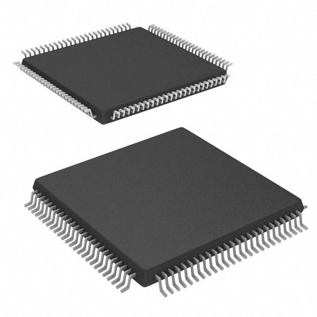
A3P250-2VQG100I ECAD Model
A3P250-2VQG100I Attributes
| Type | Description | Select |
|---|---|---|
| Rohs Code | Yes | |
| Part Life Cycle Code | Transferred | |
| Supply Voltage-Nom | 1.5 V | |
| Number of Equivalent Gates | 250000 | |
| Number of CLBs | 6144 | |
| Programmable Logic Type | FIELD PROGRAMMABLE GATE ARRAY | |
| Temperature Grade | INDUSTRIAL | |
| Package Shape | SQUARE | |
| Technology | CMOS | |
| Organization | 6144 CLBS, 250000 GATES | |
| Clock Frequency-Max | 350 MHz | |
| Supply Voltage-Max | 1.575 V | |
| Supply Voltage-Min | 1.425 V | |
| JESD-30 Code | S-PQFP-G100 | |
| Qualification Status | Not Qualified | |
| JESD-609 Code | e3 | |
| Moisture Sensitivity Level | 3 | |
| Operating Temperature-Max | 100 °C | |
| Operating Temperature-Min | -40 °C | |
| Number of Terminals | 100 | |
| Package Body Material | PLASTIC/EPOXY | |
| Package Code | TFQFP | |
| Package Shape | SQUARE | |
| Package Style | FLATPACK, THIN PROFILE, FINE PITCH | |
| Surface Mount | YES | |
| Terminal Finish | MATTE TIN | |
| Terminal Form | GULL WING | |
| Terminal Pitch | 500 µm | |
| Terminal Position | QUAD | |
| Width | 14 mm | |
| Length | 14 mm | |
| Seated Height-Max | 1.2 mm | |
| Ihs Manufacturer | MICROSEMI CORP | |
| Package Description | TFQFP, | |
| Reach Compliance Code | compliant | |
| HTS Code | 8542.39.00.01 |
A3P250-2VQG100I Datasheet Download
A3P250-2VQG100I Overview
The A3P250-2VQG100I is a Field Programmable Gate Array (FPGA) chip from the A3P family of Altera Corporation. It is based on the low-power Arria III GX architecture and is manufactured using a TSMC 0.13µm CMOS process.
The A3P250-2VQG100I has a total of 250,000 logic elements, which are divided into four distinct types: logic elements (LEs), memory blocks, embedded multipliers and digital signal processing (DSP) blocks. The LEs are capable of implementing combinational logic, while the memory blocks can store up to 16Kbits of data. The embedded multipliers can be used to perform arithmetic operations, and the DSP blocks can be used to perform complex digital signal processing functions.
The A3P250-2VQG100I has a maximum operating frequency of 200MHz and a total of 2,048 user I/Os. It also features a wide range of configurable I/Os, including LVDS, LVPECL, SSTL, HSTL, and PCI Express.
The A3P250-2VQG100I is suitable for a wide range of applications, including high-speed networking, communications, image processing, medical imaging, automotive, and industrial automation. It is also suitable for applications that require low power consumption, such as portable and battery-powered devices.
In summary, the A3P250-2VQG100I is a low-power FPGA chip from the Arria III GX family of Altera Corporation. It features 250,000 logic elements, 2,048 user I/Os, and a maximum operating frequency of 200MHz. It is suitable for a wide range of applications, including high-speed networking, communications, image processing, medical imaging, automotive, and industrial automation.
You May Also Be Interested In

5,042 In Stock
Pricing (USD)
| QTY | Unit Price | Ext Price |
|---|---|---|
| 1+ | $17.8469 | $17.8469 |
| 10+ | $17.6550 | $176.5498 |
| 100+ | $16.6955 | $1,669.5474 |
| 1000+ | $15.7360 | $7,867.9820 |
| 10000+ | $14.3927 | $14,392.6500 |
| The price is for reference only, please refer to the actual quotation! | ||