
Microchip Technology Inc
A3P250-2VQG100
A3P250-2VQG100 ECAD Model
A3P250-2VQG100 Attributes
| Type | Description | Select |
|---|---|---|
| Rohs Code | Yes | |
| Part Life Cycle Code | Transferred | |
| Supply Voltage-Nom | 1.5 V | |
| Number of Equivalent Gates | 250000 | |
| Number of CLBs | 6144 | |
| Programmable Logic Type | FIELD PROGRAMMABLE GATE ARRAY | |
| Temperature Grade | COMMERCIAL | |
| Package Shape | SQUARE | |
| Technology | CMOS | |
| Organization | 6144 CLBS, 250000 GATES | |
| Clock Frequency-Max | 350 MHz | |
| Supply Voltage-Max | 1.575 V | |
| Supply Voltage-Min | 1.425 V | |
| JESD-30 Code | S-PQFP-G100 | |
| Qualification Status | Not Qualified | |
| JESD-609 Code | e3 | |
| Moisture Sensitivity Level | 3 | |
| Operating Temperature-Max | 85 °C | |
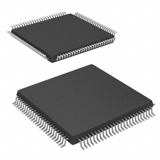
| Number of Terminals | 100 | |
| Package Body Material | PLASTIC/EPOXY | |
| Package Code | TFQFP | |
| Package Shape | SQUARE | |
| Package Style | FLATPACK, THIN PROFILE, FINE PITCH | |
| Surface Mount | YES | |
| Terminal Finish | MATTE TIN | |
| Terminal Form | GULL WING | |
| Terminal Pitch | 500 µm | |
| Terminal Position | QUAD | |
| Width | 14 mm | |
| Length | 14 mm | |
| Seated Height-Max | 1.2 mm | |
| Ihs Manufacturer | MICROSEMI CORP | |
| Package Description | TFQFP, | |
| Reach Compliance Code | compliant | |
| HTS Code | 8542.39.00.01 |
A3P250-2VQG100 Datasheet Download
A3P250-2VQG100 Overview
The A3P250-2VQG100 is an FPGA chip model developed by Altera Corporation. It is a member of the A3P family, which are low-cost, low-power, high-density FPGAs. This particular chip model is a 2-channel device that features 250K logic elements and up to 6.7Mb of embedded memory. It is designed for applications that require low-cost, low-power, and high-density FPGAs.
The chip has a power consumption of only 0.8W at 3.3V and is available in a small, 100-pin VQG package. It features a wide range of configurable I/O, including LVDS, LVCMOS, and LVTTL. It also supports high-speed transceiver support and includes a variety of I/O protection features.
The A3P250-2VQG100 is suitable for a wide range of applications, such as industrial automation, medical imaging, and consumer electronics. It is also suitable for communications, automotive, and aerospace applications, as well as for applications requiring high-speed data transfer and high-density logic.
In summary, the A3P250-2VQG100 is a low-cost, low-power, high-density FPGA chip model developed by Altera Corporation. It features 250K logic elements and up to 6.7Mb of embedded memory, and is available in a 100-pin VQG package. It is suitable for a wide range of applications, including industrial automation, medical imaging, consumer electronics, communications, automotive, and aerospace applications.
You May Also Be Interested In

2,450 In Stock
Pricing (USD)
| QTY | Unit Price | Ext Price |
|---|---|---|
| 1+ | $15.2760 | $15.2760 |
| 10+ | $15.1117 | $151.1174 |
| 100+ | $14.2904 | $1,429.0446 |
| 1000+ | $13.4692 | $6,734.5780 |
| 10000+ | $12.3194 | $12,319.3500 |
| The price is for reference only, please refer to the actual quotation! | ||