
Microchip Technology Inc
A3P250-1FGG144I
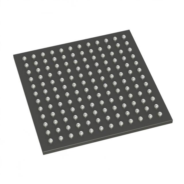
A3P250-1FGG144I ECAD Model
A3P250-1FGG144I Attributes
| Type | Description | Select |
|---|---|---|
| Rohs Code | Yes | |
| Part Life Cycle Code | Transferred | |
| Supply Voltage-Nom | 1.5 V | |
| Number of Equivalent Gates | 250000 | |
| Number of CLBs | 6144 | |
| Programmable Logic Type | FIELD PROGRAMMABLE GATE ARRAY | |
| Temperature Grade | INDUSTRIAL | |
| Package Shape | SQUARE | |
| Technology | CMOS | |
| Organization | 6144 CLBS, 250000 GATES | |
| Clock Frequency-Max | 350 MHz | |
| Supply Voltage-Max | 1.575 V | |
| Supply Voltage-Min | 1.425 V | |
| JESD-30 Code | S-PBGA-B144 | |
| Qualification Status | Not Qualified | |
| JESD-609 Code | e1 | |
| Moisture Sensitivity Level | 3 | |
| Operating Temperature-Max | 100 °C | |
| Operating Temperature-Min | -40 °C | |
| Peak Reflow Temperature (Cel) | 260 | |
| Time@Peak Reflow Temperature-Max (s) | 30 | |
| Number of Terminals | 144 | |
| Package Body Material | PLASTIC/EPOXY | |
| Package Code | LBGA | |
| Package Shape | SQUARE | |
| Package Style | GRID ARRAY, LOW PROFILE | |
| Surface Mount | YES | |
| Terminal Finish | TIN SILVER COPPER | |
| Terminal Form | BALL | |
| Terminal Pitch | 1 mm | |
| Terminal Position | BOTTOM | |
| Width | 13 mm | |
| Length | 13 mm | |
| Seated Height-Max | 1.55 mm | |
| Ihs Manufacturer | MICROSEMI CORP | |
| Package Description | LBGA, | |
| Reach Compliance Code | compliant | |
| HTS Code | 8542.39.00.01 |
A3P250-1FGG144I Datasheet Download
A3P250-1FGG144I Overview
The A3P250-1FGG144I is a Field Programmable Gate Array (FPGA) chip model that is manufactured by Actel Corporation. It is a low-cost and reliable FPGA solution that is suitable for a wide range of applications.
The A3P250-1FGG144I is a single-chip FPGA that has the capacity to store up to 250,000 gates in its internal memory. It has a total of 144 I/O pins, with 32 of them being dedicated for JTAG programming. It is also equipped with a dedicated clock signal for JTAG programming. It has a total power dissipation of 1.5W and an operating temperature range of -40°C to +85°C.
This FPGA chip model is ideal for applications that require low power consumption and reliable performance. It is suitable for use in embedded systems, consumer electronics, automotive, industrial, medical and communications applications. It is also suitable for use in applications that require programmable logic, such as data acquisition, signal processing, image processing and control systems.
The A3P250-1FGG144I is a cost-effective and reliable FPGA solution that is suitable for a wide range of applications. It has the capacity to store up to 250,000 gates in its internal memory and is equipped with a dedicated clock signal for JTAG programming. It is suitable for use in embedded systems, consumer electronics, automotive, industrial, medical and communications applications.
You May Also Be Interested In

4,619 In Stock
Pricing (USD)
| QTY | Unit Price | Ext Price |
|---|---|---|
| 1+ | $19.7239 | $19.7239 |
| 10+ | $19.5118 | $195.1182 |
| 100+ | $18.4514 | $1,845.1395 |
| 1000+ | $17.3910 | $8,695.4850 |
| 10000+ | $15.9064 | $15,906.3750 |
| The price is for reference only, please refer to the actual quotation! | ||