
Microchip Technology Inc
A3P125-2PQG208I
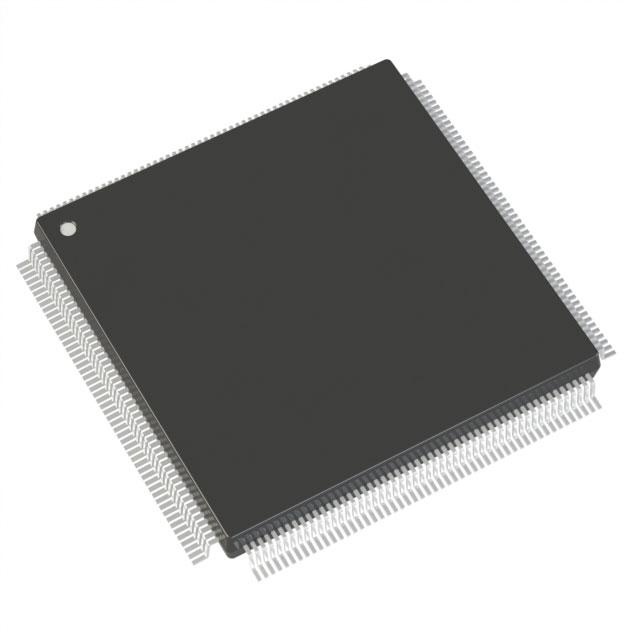
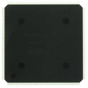
A3P125-2PQG208I ECAD Model
A3P125-2PQG208I Attributes
| Type | Description | Select |
|---|---|---|
| Rohs Code | Yes | |
| Part Life Cycle Code | Transferred | |
| Supply Voltage-Nom | 1.5 V | |
| Number of Equivalent Gates | 125000 | |
| Number of CLBs | 3072 | |
| Programmable Logic Type | FIELD PROGRAMMABLE GATE ARRAY | |
| Temperature Grade | INDUSTRIAL | |
| Package Shape | SQUARE | |
| Technology | CMOS | |
| Organization | 3072 CLBS, 125000 GATES | |
| Clock Frequency-Max | 350 MHz | |
| Supply Voltage-Max | 1.575 V | |
| Supply Voltage-Min | 1.425 V | |
| JESD-30 Code | S-PQFP-G208 | |
| Qualification Status | Not Qualified | |
| JESD-609 Code | e3 | |
| Moisture Sensitivity Level | 3 | |
| Operating Temperature-Max | 100 °C | |
| Operating Temperature-Min | -40 °C | |
| Peak Reflow Temperature (Cel) | 245 | |
| Time@Peak Reflow Temperature-Max (s) | 30 | |
| Number of Terminals | 208 | |
| Package Body Material | PLASTIC/EPOXY | |
| Package Code | FQFP | |
| Package Shape | SQUARE | |
| Package Style | FLATPACK, FINE PITCH | |
| Surface Mount | YES | |
| Terminal Finish | MATTE TIN | |
| Terminal Form | GULL WING | |
| Terminal Pitch | 500 µm | |
| Terminal Position | QUAD | |
| Width | 28 mm | |
| Length | 28 mm | |
| Seated Height-Max | 4.1 mm | |
| Ihs Manufacturer | MICROSEMI CORP | |
| Package Description | FQFP, | |
| Reach Compliance Code | compliant | |
| HTS Code | 8542.39.00.01 |
A3P125-2PQG208I Datasheet Download
A3P125-2PQG208I Overview
The A3P125-2PQG208I is a Field Programmable Gate Array (FPGA) chip from the A3P family of Altera Corporation. It is a high-performance, low-power FPGA with a maximum operating frequency of 250 MHz. It has 125K logic elements, 4,096 Kbits of embedded memory, and 8,192 Kbits of distributed memory. It has two power supply pins, with a core voltage of 1.0V and I/O voltage of 2.5V. It has a total of 208 I/O pins, including four dedicated clock pins, four dedicated JTAG pins, and four dedicated configuration pins.
This chip is designed for a wide range of applications, including digital signal processing (DSP), embedded systems, and industrial automation. It is ideal for applications that require high-speed data transfer, such as video and audio processing, image processing, and communication systems. It also supports a variety of peripherals, such as Ethernet, USB, and CAN.
The A3P125-2PQG208I has a high-speed serial interface, which allows for fast data transfer. It also has a low-power design, which makes it suitable for battery-operated applications. The chip also supports a variety of programming languages, such as Verilog and VHDL, which makes it easy to program and debug. In addition, it has a reliable and secure design, which makes it suitable for applications that require high levels of security.
Overall, the A3P125-2PQG208I is a high-performance, low-power FPGA chip that is suitable for a wide range of applications. It has a high-speed serial interface, low-power design, and reliable and secure design. It is also easy to program and debug, making it an ideal choice for many applications.
You May Also Be Interested In

5,713 In Stock
Pricing (USD)
| QTY | Unit Price | Ext Price |
|---|---|---|
| 1+ | $18.5725 | $18.5725 |
| 10+ | $18.3728 | $183.7277 |
| 100+ | $17.3742 | $1,737.4248 |
| 1000+ | $16.3757 | $8,187.8640 |
| 10000+ | $14.9778 | $14,977.8000 |
| The price is for reference only, please refer to the actual quotation! | ||