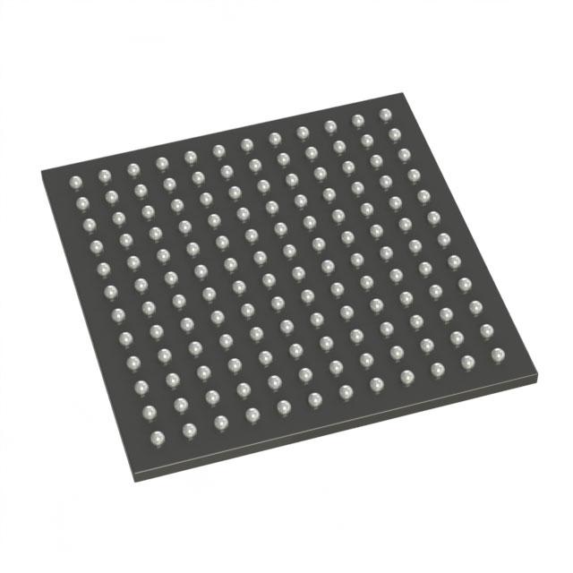
Microchip Technology Inc
A3P125-2FG144
A3P125-2FG144 ECAD Model
A3P125-2FG144 Attributes
| Type | Description | Select |
|---|---|---|
| Rohs Code | No | |
| Part Life Cycle Code | Transferred | |
| Supply Voltage-Nom | 1.5 V | |
| Number of Equivalent Gates | 125000 | |
| Number of CLBs | 3072 | |
| Programmable Logic Type | FIELD PROGRAMMABLE GATE ARRAY | |
| Temperature Grade | COMMERCIAL | |
| Package Shape | SQUARE | |
| Technology | CMOS | |
| Organization | 3072 CLBS, 125000 GATES | |
| Clock Frequency-Max | 350 MHz | |
| Supply Voltage-Max | 1.575 V | |
| Supply Voltage-Min | 1.425 V | |
| JESD-30 Code | S-PBGA-B144 | |
| Qualification Status | Not Qualified | |
| JESD-609 Code | e0 | |
| Moisture Sensitivity Level | 3 | |
| Operating Temperature-Max | 85 °C | |
| Number of Terminals | 144 | |
| Package Body Material | PLASTIC/EPOXY | |
| Package Code | LBGA | |
| Package Shape | SQUARE | |
| Package Style | GRID ARRAY, LOW PROFILE | |
| Surface Mount | YES | |
| Terminal Finish | TIN LEAD SILVER | |
| Terminal Form | BALL | |
| Terminal Pitch | 1 mm | |
| Terminal Position | BOTTOM | |
| Width | 13 mm | |
| Length | 13 mm | |
| Seated Height-Max | 1.55 mm | |
| Ihs Manufacturer | MICROSEMI CORP | |
| Package Description | LBGA, | |
| Reach Compliance Code | unknown | |
| HTS Code | 8542.39.00.01 |
A3P125-2FG144 Datasheet Download
A3P125-2FG144 Overview
The A3P125-2FG144 is a programmable logic device from the A3P family of Xilinx FPGAs. This device is based on the Artix-7 architecture, which offers the highest performance and lowest power consumption of any FPGA in the Xilinx range. It features 144 user-programmable logic blocks, each containing four 6-input Look-Up Tables (LUTs) and 16 Flip-Flops, as well as two dedicated DSP blocks, two dedicated Block RAM blocks, and sixteen dedicated I/O blocks. The device also provides up to 8Mbits of embedded memory, and up to 656 user-programmable I/O pins.
This FPGA is suitable for a wide range of applications, including consumer electronics, embedded systems, automotive, industrial control, medical imaging, and defense. It is capable of handling high-speed data processing tasks, such as image processing, video processing, signal processing, and communication. It is also suitable for implementing complex logic functions, such as control logic, signal routing, and system integration.
The A3P125-2FG144 is a cost-effective solution for customers who require a high-performance FPGA with a wide range of features. It is available in a variety of packages, including a 144-pin TQFP, a 176-pin BGA, and a 256-pin BGA. It is also compatible with a wide range of development tools, such as the Xilinx Vivado Design Suite, and can be programmed using the Xilinx ISE Design Suite.
You May Also Be Interested In
3,619 In Stock
Pricing (USD)
| QTY | Unit Price | Ext Price |
|---|---|---|
| 1+ | $23.0025 | $23.0025 |
| 10+ | $22.7552 | $227.5519 |
| 100+ | $21.5185 | $2,151.8493 |
| 1000+ | $20.2818 | $10,140.8990 |
| 10000+ | $18.5504 | $18,550.4250 |
| The price is for reference only, please refer to the actual quotation! | ||

