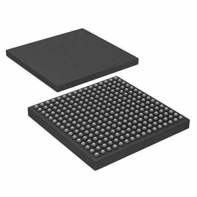
Microchip Technology Inc
A3P1000L-1FGG256I
A3P1000L-1FGG256I ECAD Model
A3P1000L-1FGG256I Attributes
| Type | Description | Select |
|---|---|---|
| Rohs Code | Yes | |
| Part Life Cycle Code | Transferred | |
| Supply Voltage-Nom | 1.2 V | |
| Number of Inputs | 177 | |
| Number of Outputs | 177 | |
| Number of Logic Cells | 24576 | |
| Number of Equivalent Gates | 1000000 | |
| Number of CLBs | 24576 | |
| Programmable Logic Type | FIELD PROGRAMMABLE GATE ARRAY | |
| Temperature Grade | INDUSTRIAL | |
| Package Shape | SQUARE | |
| Technology | CMOS | |
| Organization | 24576 CLBS, 1000000 GATES | |
| Clock Frequency-Max | 350 MHz | |
| Power Supplies | 1.5/3.3 V | |
| Supply Voltage-Max | 1.575 V | |
| Supply Voltage-Min | 1.14 V | |
| JESD-30 Code | S-PBGA-B256 | |
| Qualification Status | Not Qualified | |
| JESD-609 Code | e1 | |
| Moisture Sensitivity Level | 3 | |
| Operating Temperature-Max | 85 °C | |
| Operating Temperature-Min | -40 °C | |
| Peak Reflow Temperature (Cel) | 260 | |
| Time@Peak Reflow Temperature-Max (s) | 40 | |
| Number of Terminals | 256 | |
| Package Body Material | PLASTIC/EPOXY | |
| Package Code | BGA | |
| Package Equivalence Code | BGA256,16X16,40 | |
| Package Shape | SQUARE | |
| Package Style | GRID ARRAY | |
| Surface Mount | YES | |
| Terminal Finish | Tin/Silver/Copper (Sn/Ag/Cu) | |
| Terminal Form | BALL | |
| Terminal Pitch | 1 mm | |
| Terminal Position | BOTTOM | |
| Width | 17 mm | |
| Length | 17 mm | |
| Seated Height-Max | 1.8 mm | |
| Ihs Manufacturer | MICROSEMI CORP | |
| Reach Compliance Code | compliant | |
| HTS Code | 8542.39.00.01 | |
| Package Description | BGA, BGA256,16X16,40 |
A3P1000L-1FGG256I Datasheet Download
A3P1000L-1FGG256I Overview
The A3P1000L-1FGG256I is a Field Programmable Gate Array (FPGA) chip from Altera. It is a low-cost, low-power device that provides a high level of integration and flexibility for a variety of applications.
The A3P1000L-1FGG256I has a total of 256 logic elements and a total of 4,096 bits of embedded memory. It also has a dedicated multiplier for fast and efficient computation. The device has a single-cycle reconfiguration, which allows for fast reconfiguration of the logic elements. It also has a dedicated phase-locked loop (PLL) and a dedicated clock management unit (CMU) for improved clock performance.
The A3P1000L-1FGG256I is ideal for applications that require high performance and low power consumption. It is suitable for a wide range of embedded applications, including automotive, industrial, healthcare, and consumer electronics. It can also be used in applications such as digital signal processing, image processing, communications, and networking.
The A3P1000L-1FGG256I is designed with a flexible architecture, allowing for easy integration with other components. It is also designed for high reliability and is RoHS compliant. The device has a wide operating temperature range of -40°C to +85°C.
In summary, the A3P1000L-1FGG256I is a low-cost, low-power, and highly integrated FPGA device that is suitable for a wide range of embedded applications. It has a single-cycle reconfiguration, a dedicated multiplier, a PLL, and a CMU for improved clock performance. It is designed with a flexible architecture for easy integration with other components, and has a wide operating temperature range.
You May Also Be Interested In
1,111 In Stock
Pricing (USD)
| QTY | Unit Price | Ext Price |
|---|---|---|
| 1+ | $254.1350 | $254.1350 |
| 10+ | $251.4023 | $2,514.0233 |
| 100+ | $237.7392 | $23,773.9158 |
| 1000+ | $224.0760 | $112,037.9940 |
| 10000+ | $204.9476 | $204,947.5500 |
| The price is for reference only, please refer to the actual quotation! | ||


