
Microchip Technology Inc
A3P1000-1FG484I
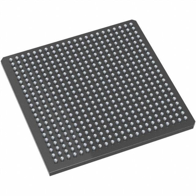
A3P1000-1FG484I ECAD Model
A3P1000-1FG484I Attributes
| Type | Description | Select |
|---|---|---|
| Rohs Code | No | |
| Part Life Cycle Code | Transferred | |
| Supply Voltage-Nom | 1.5 V | |
| Number of Equivalent Gates | 1000000 | |
| Number of CLBs | 24576 | |
| Programmable Logic Type | FIELD PROGRAMMABLE GATE ARRAY | |
| Temperature Grade | INDUSTRIAL | |
| Package Shape | SQUARE | |
| Technology | CMOS | |
| Organization | 24576 CLBS, 1000000 GATES | |
| Clock Frequency-Max | 350 MHz | |
| Supply Voltage-Max | 1.575 V | |
| Supply Voltage-Min | 1.425 V | |
| JESD-30 Code | S-PBGA-B484 | |
| Qualification Status | Not Qualified | |
| JESD-609 Code | e0 | |
| Operating Temperature-Max | 100 °C | |
| Operating Temperature-Min | -40 °C | |
| Number of Terminals | 484 | |
| Package Body Material | PLASTIC/EPOXY | |
| Package Code | BGA | |
| Package Shape | SQUARE | |
| Package Style | GRID ARRAY | |
| Surface Mount | YES | |
| Terminal Finish | TIN LEAD | |
| Terminal Form | BALL | |
| Terminal Pitch | 1 mm | |
| Terminal Position | BOTTOM | |
| Width | 23 mm | |
| Length | 23 mm | |
| Seated Height-Max | 2.44 mm | |
| Ihs Manufacturer | MICROSEMI CORP | |
| Package Description | BGA, | |
| Reach Compliance Code | unknown | |
| HTS Code | 8542.39.00.01 |
A3P1000-1FG484I Datasheet Download
A3P1000-1FG484I Overview
The A3P1000-1FG484I is a high-performance FPGA chip manufactured by Lattice Semiconductor. It is designed for a wide range of applications, from consumer electronics to industrial automation.
The A3P1000-1FG484I is a low-power, low-cost FPGA chip that is ideal for applications such as digital signal processing, embedded systems, and communication systems. It has a total of 4,848 logic cells, and can be configured in a variety of ways, including 16-bit and 32-bit data widths. It has up to 256 Kbits of embedded RAM and up to 1.2 Mbits of embedded ROM.
The A3P1000-1FG484I also features an array of I/O ports, including 4 differential pairs of LVDS I/O, 24 single-ended I/O, and 16 dedicated LVDS I/O. It is also equipped with a number of dedicated peripherals, including a Clock Manager, a PLL, a JTAG controller, and a Multi-Purpose I/O Block.
The A3P1000-1FG484I is designed to operate at a maximum frequency of up to 250 MHz, and is suitable for a wide range of applications, including industrial automation, automotive, medical, and consumer electronics. It is also well-suited for a variety of embedded applications, such as motion control, motor control, and image processing. The A3P1000-1FG484I is available in a variety of packages, including a 484-pin BGA and a 256-pin FBGA.
You May Also Be Interested In

2,642 In Stock
Pricing (USD)
| QTY | Unit Price | Ext Price |
|---|---|---|
| 1+ | $137.4007 | $137.4007 |
| 10+ | $135.9233 | $1,359.2328 |
| 100+ | $128.5361 | $12,853.6149 |
| 1000+ | $121.1490 | $60,574.5070 |
| 10000+ | $110.8070 | $110,807.0250 |
| The price is for reference only, please refer to the actual quotation! | ||