
Microchip Technology Inc
A3P030-2QNG68I
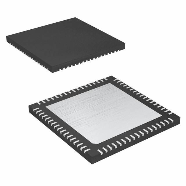
A3P030-2QNG68I ECAD Model
A3P030-2QNG68I Attributes
| Type | Description | Select |
|---|---|---|
| Rohs Code | Yes | |
| Part Life Cycle Code | Transferred | |
| Supply Voltage-Nom | 1.5 V | |
| Number of Equivalent Gates | 30000 | |
| Number of CLBs | 768 | |
| Programmable Logic Type | FIELD PROGRAMMABLE GATE ARRAY | |
| Temperature Grade | INDUSTRIAL | |
| Package Shape | SQUARE | |
| Technology | CMOS | |
| Organization | 768 CLBS, 30000 GATES | |
| Supply Voltage-Max | 1.575 V | |
| Supply Voltage-Min | 1.425 V | |
| JESD-30 Code | S-XQCC-N68 | |
| Qualification Status | Not Qualified | |
| Moisture Sensitivity Level | 3 | |
| Operating Temperature-Max | 100 °C | |
| Operating Temperature-Min | -40 °C | |
| Number of Terminals | 68 | |
| Package Body Material | UNSPECIFIED | |
| Package Code | HVQCCN | |
| Package Shape | SQUARE | |
| Package Style | CHIP CARRIER, HEAT SINK/SLUG, VERY THIN PROFILE | |
| Surface Mount | YES | |
| Terminal Form | NO LEAD | |
| Terminal Pitch | 400 µm | |
| Terminal Position | QUAD | |
| Width | 8 mm | |
| Length | 8 mm | |
| Seated Height-Max | 1 mm | |
| Ihs Manufacturer | MICROSEMI CORP | |
| Package Description | HVQCCN, | |
| Reach Compliance Code | compliant | |
| HTS Code | 8542.39.00.01 |
A3P030-2QNG68I Datasheet Download
A3P030-2QNG68I Overview
The A3P030-2QNG68I is a Field Programmable Gate Array (FPGA) chip produced by Lattice Semiconductor. It is a low-power, low-cost device with a wide range of applications.
The A3P030-2QNG68I is a low-power, low-cost FPGA chip with a small form factor. It is based on the Lattice CrossLink architecture and has a total of 30,000 logic elements and 16,000 memory blocks. It also has a wide range of I/O options, including LVDS, LVCMOS, and SGMII. It supports various standards such as USB 2.0, PCIe Gen2, and Ethernet. It also supports a wide range of clock speeds, from 25MHz to 200MHz.
The A3P030-2QNG68I is suitable for a wide range of applications, including industrial automation, medical imaging, automotive, and communications. It can be used for high-speed data acquisition, signal processing, and control applications. It is also suitable for applications that require low power consumption and a small form factor.
In conclusion, the A3P030-2QNG68I is a low-power, low-cost FPGA chip with a wide range of I/O options and clock speeds. It is suitable for a wide range of applications, including industrial automation, medical imaging, automotive, and communications.
You May Also Be Interested In

3,670 In Stock
Pricing (USD)
| QTY | Unit Price | Ext Price |
|---|---|---|
| 1+ | $6.0962 | $6.0962 |
| 10+ | $6.0307 | $60.3069 |
| 100+ | $5.7029 | $570.2937 |
| 1000+ | $5.3752 | $2,687.5910 |
| 10000+ | $4.9163 | $4,916.3250 |
| The price is for reference only, please refer to the actual quotation! | ||