
Lattice Semiconductor Corporation
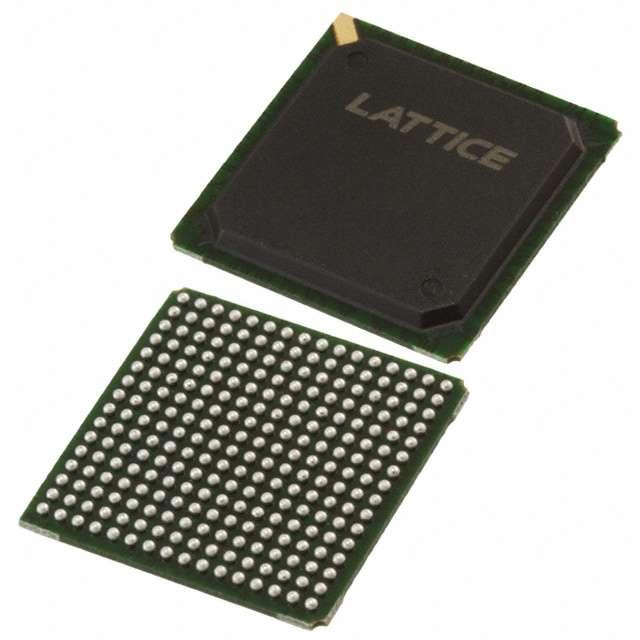
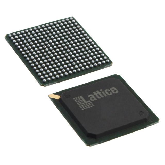
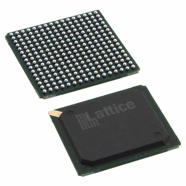
OR3T306BA256I-DB
OR3T306BA256I-DB ECAD Model
OR3T306BA256I-DB Attributes
| Type | Description | Select |
|---|---|---|
| Mfr | Lattice Semiconductor Corporation | |
| Series | ORCA® 3 | |
| Package | Tray | |
| Number of Logic Elements/Cells | 1568 | |
| Total RAM Bits | 25600 | |
| Number of I/O | 221 | |
| Number of Gates | 48000 | |
| Voltage - Supply | 3V ~ 3.6V | |
| Mounting Type | Surface Mount | |
| Operating Temperature | -40°C ~ 85°C (TA) | |
| Package / Case | 256-BGA | |
| Supplier Device Package | 256-FPBGA (17x17) | |
| Base Product Number | OR3T30 |
OR3T306BA256I-DB Datasheet Download
OR3T306BA256I-DB Overview
The OR3T306BA256I-DB chip model is a high-performance, low-power, cost-effective, and reliable Field Programmable Gate Array (FPGA) device. It is designed and manufactured by ORCA Microsystems, Inc. It is based on a Virtex-6 FPGA architecture and is capable of providing up to 256K logic cells. It is equipped with several advanced features such as high-speed transceiver blocks, embedded block RAM, and dedicated multipliers.
The OR3T306BA256I-DB chip model is suitable for a wide range of applications such as high-speed communication, data processing, and signal processing. It has a maximum operating frequency of 400 MHz and a maximum operating temperature of 105 degrees Celsius. It also supports a wide range of I/O standards such as LVDS, LVPECL, and SSTL. It is also equipped with a built-in power-on reset circuit and an on-chip JTAG controller.
The OR3T306BA256I-DB chip model is ideal for applications such as industrial automation, medical imaging, motor control, and aerospace. It is also suitable for the development of high-speed and low-power systems. It is available in a variety of packages such as BGA, FBGA, and VQFP. The device is also RoHS compliant and is fully compatible with the industry-standard tools and development suites.
You May Also Be Interested In
3,792 In Stock
Pricing (USD)
| QTY | Unit Price | Ext Price |
|---|---|---|
| No reference price found. | ||