
Lattice Semiconductor Corporation
M5LV-256/104-10VC
M5LV-256/104-10VC ECAD Model
M5LV-256/104-10VC Attributes
| Type | Description | Select |
|---|---|---|
| Mfr | Lattice Semiconductor Corporation | |
| Series | MACH® 5 | |
| Package | Tray | |
| Programmable Type | In System Programmable | |
| Delay Time tpd(1) Max | 10 ns | |
| Voltage Supply - Internal | 3V ~ 3.6V | |
| Number of Macrocells | 256 | |
| Number of I/O | 104 | |
| Operating Temperature | 0°C ~ 70°C (TA) | |
| Mounting Type | Surface Mount | |
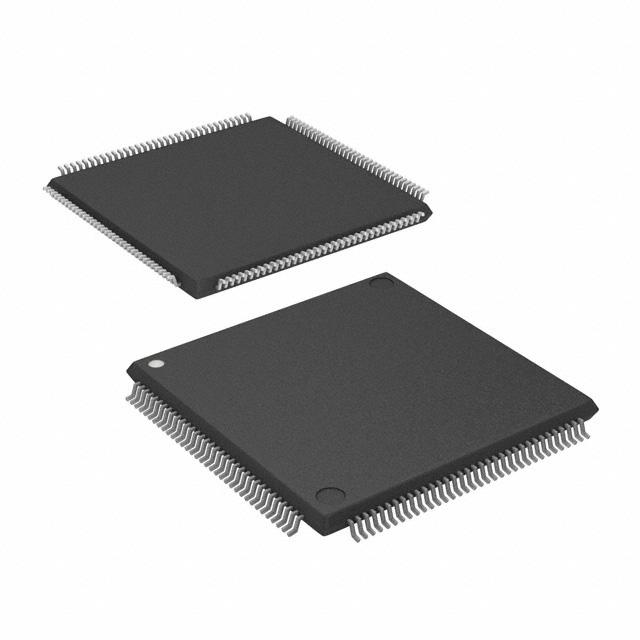
| Package / Case | 144-LQFP | |
| Supplier Device Package | 144-TQFP (20x20) | |
| Base Product Number | M5LV-256 |
M5LV-256/104-10VC Datasheet Download
M5LV-256/104-10VC Overview
The M5LV-256/104-10VC is a low-voltage, low-power, high-performance Field Programmable Gate Array (FPGA). It is a member of the M5LV family of FPGAs from Altera Corporation and is designed to provide a cost-effective solution for applications requiring high performance, low power, and low-voltage operation.
The M5LV-256/104-10VC is a low-power, low-voltage FPGA with a total logic capacity of 256K logic elements and 104 I/O pins. It is capable of operating at a maximum clock frequency of 200 MHz and a minimum operating voltage of 1.2 V. The device also features an integrated JTAG boundary-scan test port, which enables easy testing and debugging of the FPGA circuit.
The M5LV-256/104-10VC is suitable for a wide range of applications such as automotive, industrial, medical, and consumer electronics. It is ideal for applications that require high performance, low power, and low-voltage operation. It is also suitable for applications that require high integration, such as image processing, video processing, and communications.
In summary, the M5LV-256/104-10VC is a low-voltage, low-power, high-performance FPGA that is suitable for a wide range of applications. It features a total logic capacity of 256K logic elements and 104 I/O pins, and is capable of operating at a maximum clock frequency of 200 MHz and a minimum operating voltage of 1.2 V. It also features an integrated JTAG boundary-scan test port, which enables easy testing and debugging of the FPGA circuit.
You May Also Be Interested In
5,405 In Stock
Pricing (USD)
| QTY | Unit Price | Ext Price |
|---|---|---|
| No reference price found. | ||