
Lattice Semiconductor Corporation
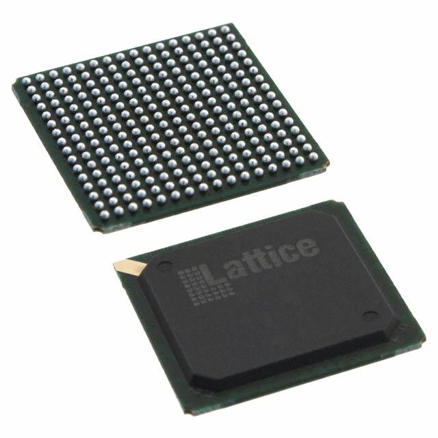
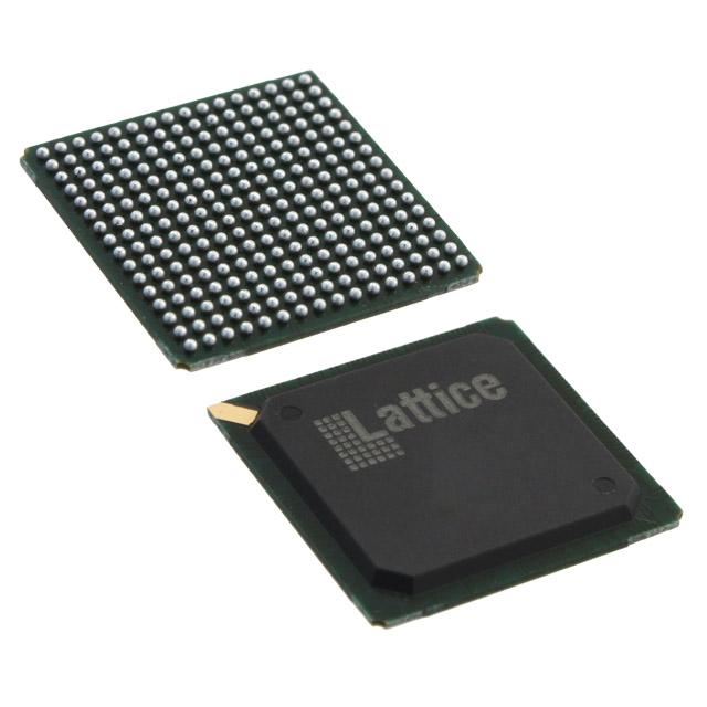
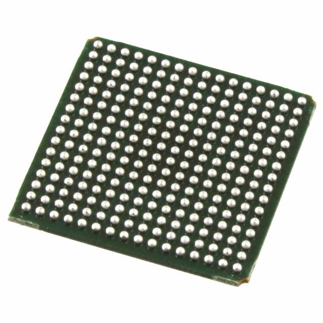
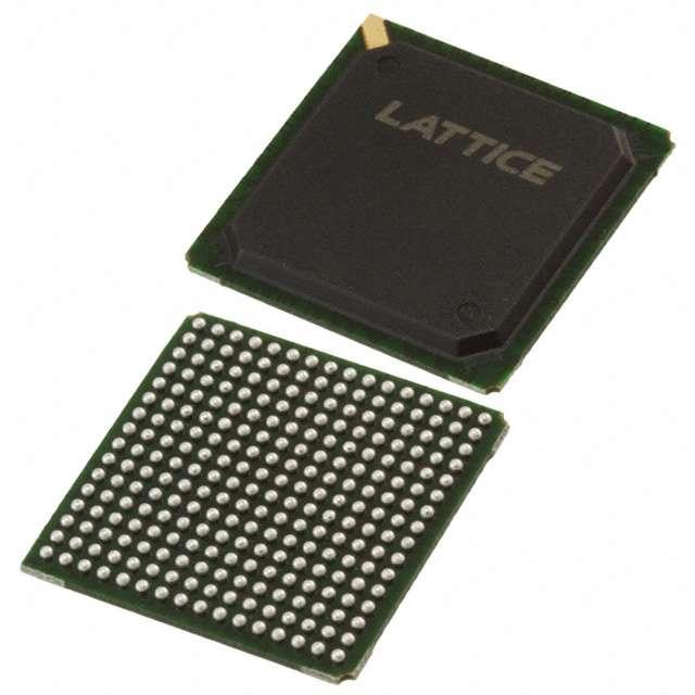
LFXP6E-4FN256C
LFXP6E-4FN256C ECAD Model
LFXP6E-4FN256C Attributes
| Type | Description | Select |
|---|---|---|
| Mfr | Lattice Semiconductor Corporation | |
| Series | XP | |
| Package | Tray | |
| Number of Logic Elements/Cells | 6000 | |
| Total RAM Bits | 73728 | |
| Number of I/O | 188 | |
| Voltage - Supply | 1.14V ~ 1.26V | |
| Mounting Type | Surface Mount | |
| Operating Temperature | 0°C ~ 85°C (TJ) | |
| Package / Case | 256-BGA | |
| Supplier Device Package | 256-FPBGA (17x17) | |
| Base Product Number | LFXP6 |
LFXP6E-4FN256C Datasheet Download
LFXP6E-4FN256C Overview
The LFXP6E-4FN256C is a low-power, low-cost, field-programmable gate array (FPGA) chip from Lattice Semiconductor. It is designed for use in a wide range of applications including digital signal processing, embedded control, industrial automation and consumer electronics.
The chip has a 4-bit 256-cell architecture, making it well suited for low-power applications. It features a low-power, low-cost, non-volatile programmable logic solution that is ideal for applications requiring a low-cost, low-power solution. The chip is also capable of supporting up to 32-bit data widths and up to 8-bit data widths.
The chip also features an integrated programmable clock generator, which allows for the generation of multiple clock frequencies. It also supports multiple clock domains, allowing for the use of multiple clock frequencies on different parts of the device.
The chip also features an integrated power-on reset circuit, allowing for the reset of the device after power-on. It also features an integrated power-down control circuit, allowing for the automatic power-down of the device when not in use.
The chip is also capable of supporting a wide range of I/O standards, including LVDS, LVCMOS, SSTL, and HSTL. It also supports a wide range of memory interfaces, including DDR, DDR2, and DDR3.
Overall, the LFXP6E-4FN256C is an ideal choice for a wide range of applications requiring a low-power, low-cost, programmable logic solution. It is a cost-effective solution for applications requiring multiple clock frequencies, multiple clock domains, and a wide range of I/O and memory interfaces.
You May Also Be Interested In
1,966 In Stock
Pricing (USD)
| QTY | Unit Price | Ext Price |
|---|---|---|
| No reference price found. | ||