

Lattice Semiconductor Corporation
LFXP6C-3QN208I
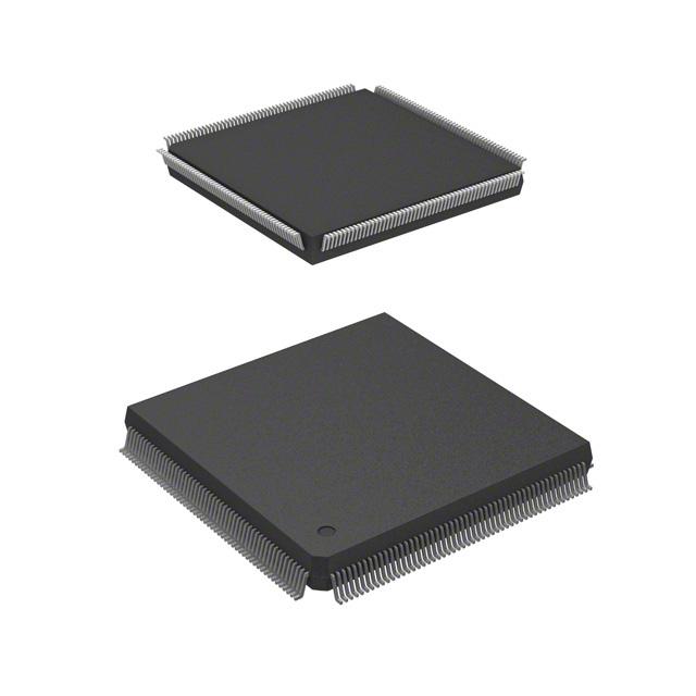
LFXP6C-3QN208I ECAD Model
LFXP6C-3QN208I Attributes
| Type | Description | Select |
|---|---|---|
| Mfr | Lattice Semiconductor Corporation | |
| Series | XP | |
| Package | Tray | |
| Number of Logic Elements/Cells | 6000 | |
| Total RAM Bits | 73728 | |
| Number of I/O | 142 | |
| Voltage - Supply | 1.71V ~ 3.465V | |
| Mounting Type | Surface Mount | |
| Operating Temperature | -40°C ~ 100°C (TJ) | |
| Package / Case | 208-BFQFP | |
| Supplier Device Package | 208-PQFP (28x28) | |
| Base Product Number | LFXP6 |
LFXP6C-3QN208I Datasheet Download
LFXP6C-3QN208I Overview
The LFXP6C-3QN208I is a low-power, low-voltage Field Programmable Gate Array (FPGA) manufactured by Lattice Semiconductor. It is based on the Lattice XP2 FPGA architecture and is designed for applications requiring low power consumption and low cost.
The LFXP6C-3QN208I has a total of 208 logic elements (LEs), with up to 32 user-configurable I/Os and a maximum clock frequency of 150MHz. It also features an embedded 8Kbit block RAM, 1Kbit user flash, and up to 24Kbits of user-configurable SRAM. The FPGA features low-power, low-voltage operation, with a core voltage range of 1.2V to 1.5V and I/O voltage range of 1.2V to 3.3V.
The LFXP6C-3QN208I is suitable for a variety of applications, including consumer electronics, industrial, automotive, medical, and communications. It is ideal for applications that require low cost, low power consumption, and small form factor, such as wearable devices, IoT devices, and industrial automation.
The LFXP6C-3QN208I is available in a small, 10x10mm, 208-pin LQFP package, and is RoHS compliant. It is also compatible with the Lattice Diamond Design Software and the Lattice iCEcube2 Design Software, making it easy to design and integrate into existing systems.
You May Also Be Interested In


4,636 In Stock
Pricing (USD)
| QTY | Unit Price | Ext Price |
|---|---|---|
| No reference price found. | ||