
Lattice Semiconductor Corporation
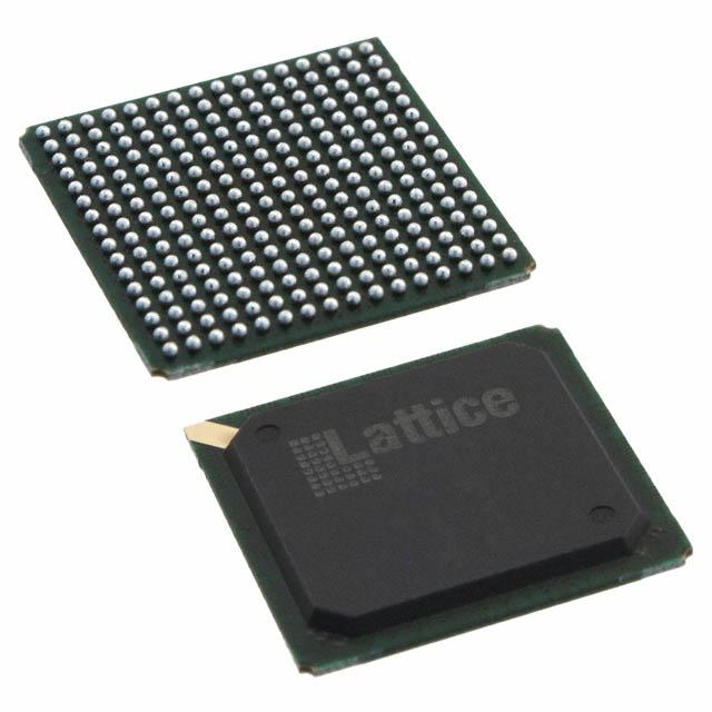
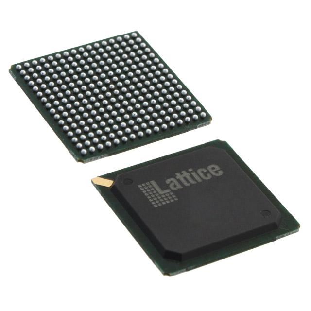
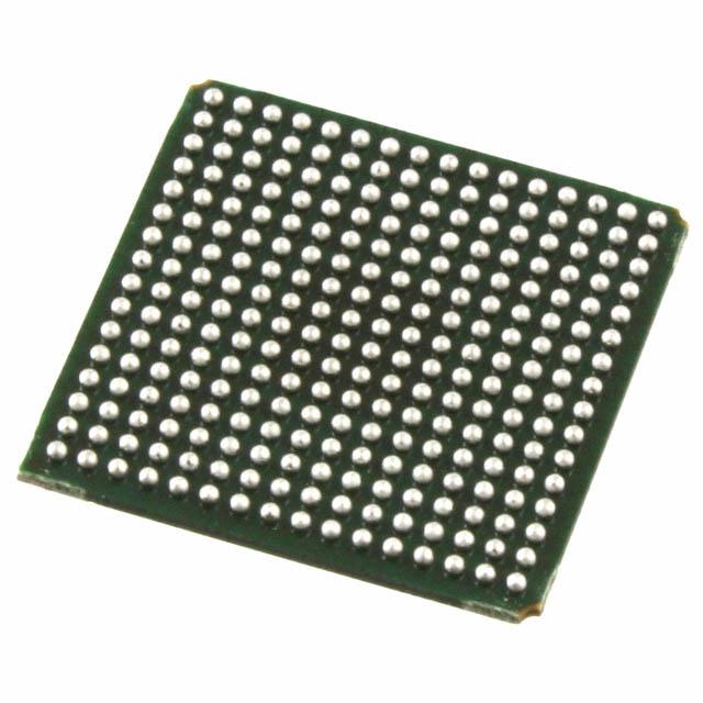
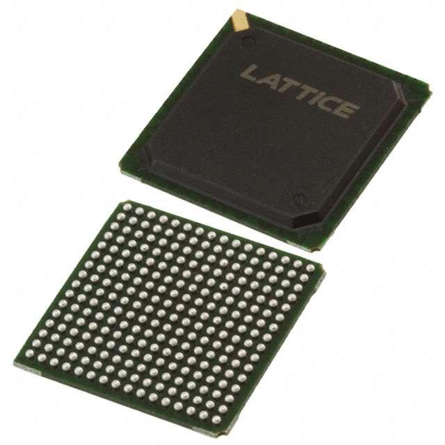
LFXP6C-3F256I
LFXP6C-3F256I ECAD Model
LFXP6C-3F256I Attributes
| Type | Description | Select |
|---|---|---|
| Mfr | Lattice Semiconductor Corporation | |
| Series | XP | |
| Package | Tray | |
| Number of Logic Elements/Cells | 6000 | |
| Total RAM Bits | 73728 | |
| Number of I/O | 188 | |
| Voltage - Supply | 1.71V ~ 3.465V | |
| Mounting Type | Surface Mount | |
| Operating Temperature | -40°C ~ 100°C (TJ) | |
| Package / Case | 256-BGA | |
| Supplier Device Package | 256-FPBGA (17x17) | |
| Base Product Number | LFXP6 |
LFXP6C-3F256I Datasheet Download
LFXP6C-3F256I Overview
The LFXP6C-3F256I is a low-power, high-performance Field Programmable Gate Array (FPGA) chip from Lattice Semiconductor Corporation. It is based on the LatticeXP2 architecture and is designed for applications requiring low power and high performance.
The LFXP6C-3F256I has 256 I/Os, up to 8K LUTs, and up to 16Kb of block RAM. It is fabricated using a 0.18um CMOS process and is packaged in a 7x7mm, 144-pin fine-pitch BGA package. The device has a maximum power dissipation of 1.5W.
The LFXP6C-3F256I is suitable for a variety of applications, including automotive, industrial, medical, and consumer. It can be used for a wide range of applications including signal processing, video processing, image processing, communications, control, and embedded systems. It has a wide range of features such as high-speed I/O, high-speed clock management, and low-power design.
The LFXP6C-3F256I is suitable for applications that require a combination of low power and high performance. It is a cost-effective solution for a wide range of applications and can be used in a variety of applications. The device is designed to be used in a wide range of applications, including automotive, industrial, medical, and consumer.
You May Also Be Interested In
1,940 In Stock
Pricing (USD)
| QTY | Unit Price | Ext Price |
|---|---|---|
| No reference price found. | ||