
Lattice Semiconductor Corporation
LFXP3C-3TN144I
LFXP3C-3TN144I ECAD Model
LFXP3C-3TN144I Attributes
| Type | Description | Select |
|---|---|---|
| Mfr | Lattice Semiconductor Corporation | |
| Series | XP | |
| Package | Tray | |
| Number of Logic Elements/Cells | 3000 | |
| Total RAM Bits | 55296 | |
| Number of I/O | 100 | |
| Voltage - Supply | 1.71V ~ 3.465V | |
| Mounting Type | Surface Mount | |
| Operating Temperature | -40°C ~ 100°C (TJ) | |
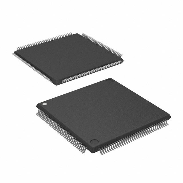
| Package / Case | 144-LQFP | |
| Supplier Device Package | 144-TQFP (20x20) | |
| Base Product Number | LFXP3 |
LFXP3C-3TN144I Datasheet Download
LFXP3C-3TN144I Overview
The LFXP3C-3TN144I is a low-power, low-cost, field-programmable gate array (FPGA) chip from Lattice Semiconductor. It is a member of the LatticeXP family of FPGAs, which are designed for low-cost, low-power applications. The LFXP3C-3TN144I is a 3.3V device with a 144-pin package. It features a total of 3,744 logic elements, including 2,976 four-input look-up tables (LUTs), 1,536 flip-flops, and 32 block RAMs. It also supports up to 16 user I/O pins and has two independent clock domains. The chip has a maximum clock frequency of 125 MHz and a maximum power consumption of 2 Watts.
The LFXP3C-3TN144I is ideal for a wide range of embedded applications, including industrial control, consumer electronics, and automotive. It is well-suited for applications that require low power consumption, small form factor, and low cost. It is also suitable for applications that require high performance and fast development cycles. The chip is compatible with various programming languages and development tools, making it easy to design and implement complex logic. The LFXP3C-3TN144I is also ideal for applications that require secure, reliable, and low-cost FPGA solutions.
You May Also Be Interested In
4,275 In Stock
Pricing (USD)
| QTY | Unit Price | Ext Price |
|---|---|---|
| No reference price found. | ||