
Lattice Semiconductor Corporation
LFXP2-30E-7FT256C
LFXP2-30E-7FT256C ECAD Model
LFXP2-30E-7FT256C Attributes
| Type | Description | Select |
|---|---|---|
| Mfr | Lattice Semiconductor Corporation | |
| Series | XP2 | |
| Package | Tray | |
| Number of LABs/CLBs | 3625 | |
| Number of Logic Elements/Cells | 29000 | |
| Total RAM Bits | 396288 | |
| Number of I/O | 201 | |
| Voltage - Supply | 1.14V ~ 1.26V | |
| Mounting Type | Surface Mount | |
| Operating Temperature | 0°C ~ 85°C (TJ) | |
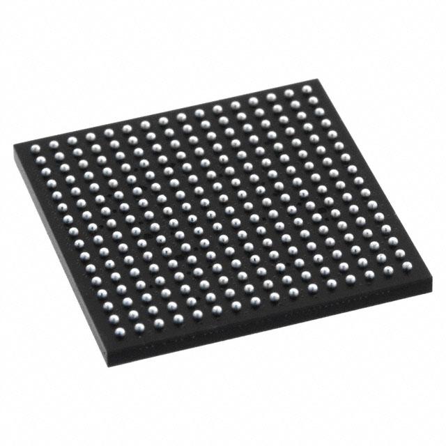
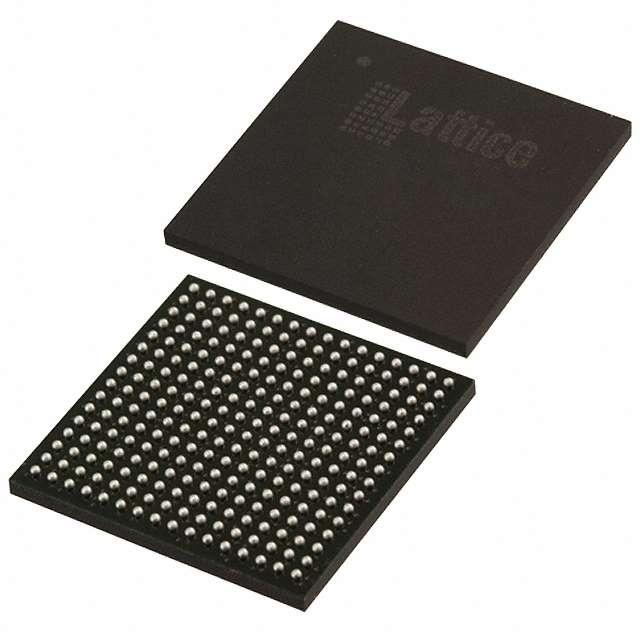
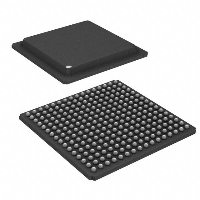
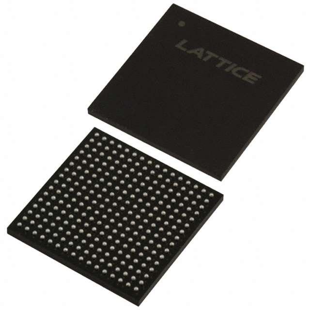
| Package / Case | 256-LBGA | |
| Supplier Device Package | 256-FTBGA (17x17) | |
| Base Product Number | LFXP2-30 |
LFXP2-30E-7FT256C Datasheet Download
LFXP2-30E-7FT256C Overview
The LFXP2-30E-7FT256C is a low-power, low-cost, low-power and low-cost FPGA chip model designed by Lattice Semiconductor. It is ideal for applications requiring high performance with minimal power consumption. The chip is based on the LatticeXP2 architecture, which is designed to reduce power consumption while providing high performance.
The LFXP2-30E-7FT256C is a 256-pin, 7-layer FPGA chip model. It has a total of 30,000 logic elements, with up to 576 Kbits of embedded SRAM and up to 4,608 Kbits of embedded flash memory. It also features a wide range of I/O capabilities, including LVDS, LVCMOS, and GPIO. It has a maximum operating frequency of up to 150MHz, and a maximum power consumption of 4.5W.
The LFXP2-30E-7FT256C is ideal for a wide range of applications, including industrial automation, medical equipment, consumer electronics, and automotive. It is suitable for applications such as image processing, video processing, and machine learning. Its low power consumption and high performance make it an ideal choice for applications requiring low power and high performance. It is also suitable for low-cost applications, making it an attractive choice for cost-sensitive applications.
You May Also Be Interested In
1,538 In Stock
Pricing (USD)
| QTY | Unit Price | Ext Price |
|---|---|---|
| No reference price found. | ||