
Lattice Semiconductor Corporation
LFXP2-30E-7FN484C
LFXP2-30E-7FN484C ECAD Model
LFXP2-30E-7FN484C Attributes
| Type | Description | Select |
|---|---|---|
| Mfr | Lattice Semiconductor Corporation | |
| Series | XP2 | |
| Package | Tray | |
| Number of LABs/CLBs | 3625 | |
| Number of Logic Elements/Cells | 29000 | |
| Total RAM Bits | 396288 | |
| Number of I/O | 363 | |
| Voltage - Supply | 1.14V ~ 1.26V | |
| Mounting Type | Surface Mount | |
| Operating Temperature | 0°C ~ 85°C (TJ) | |
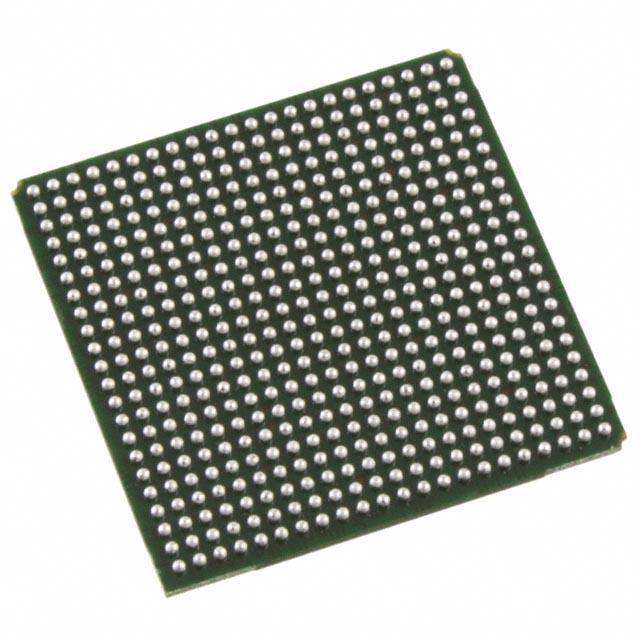
| Package / Case | 484-BBGA | |
| Supplier Device Package | 484-FPBGA (23x23) | |
| Base Product Number | LFXP2-30 |
LFXP2-30E-7FN484C Datasheet Download
LFXP2-30E-7FN484C Overview
The LFXP2-30E-7FN484C is a low-power, mid-range, field-programmable gate array (FPGA) from Lattice Semiconductor Corporation. It is part of the LatticeXP2 family, and is designed for a wide range of applications. This FPGA is ideal for applications requiring a cost-effective and low-power solution.
The LFXP2-30E-7FN484C features an array of programmable logic blocks, which can be used to implement complex digital designs. It also includes up to 7,000 logic cells, up to 7,000 flip-flops, up to 4,000 I/O pins, and up to 8,000 RAM blocks. It also supports up to 10 dedicated high-speed SERDES lanes, as well as up to 28 dedicated LVDS I/O pairs. The device also includes an integrated high-speed differential clock buffer, and a low-power, low-noise PLL.
The LFXP2-30E-7FN484C is suitable for a wide range of applications, including industrial automation, medical devices, consumer electronics, automotive, aerospace, and communications. It is also suitable for use in high-speed, low-power designs. It is available in a 7x7 mm, 484-pin BGA package, and is RoHS compliant.
Overall, the LFXP2-30E-7FN484C is a low-power, mid-range FPGA from Lattice Semiconductor Corporation. It features an array of programmable logic blocks, up to 7,000 logic cells, up to 7,000 flip-flops, up to 4,000 I/O pins, and up to 8,000 RAM blocks. It is suitable for a wide range of applications, including industrial automation, medical devices, consumer electronics, automotive, aerospace, and communications.
You May Also Be Interested In
5,640 In Stock
Pricing (USD)
| QTY | Unit Price | Ext Price |
|---|---|---|
| 1+ | $160.7578 | $160.7578 |
| 10+ | $159.0293 | $1,590.2927 |
| 100+ | $150.3864 | $15,038.6373 |
| 1000+ | $141.7435 | $70,871.7390 |
| 10000+ | $129.6434 | $129,643.4250 |
| The price is for reference only, please refer to the actual quotation! | ||