
Lattice Semiconductor Corporation
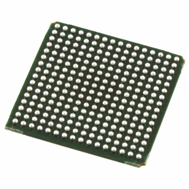
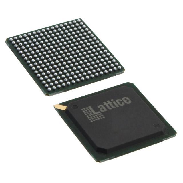
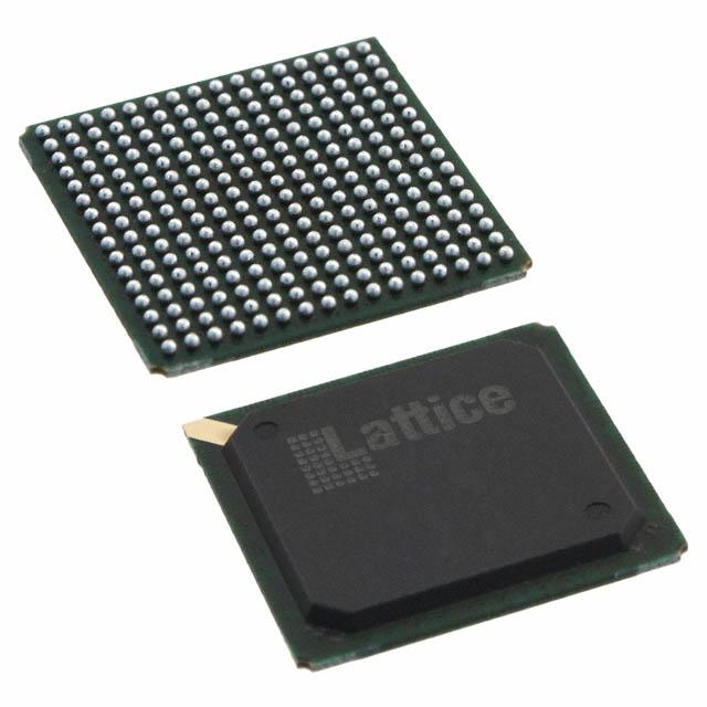
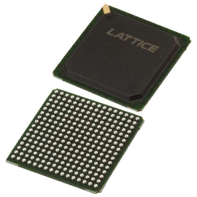
LFX200EB-03FN256C
LFX200EB-03FN256C ECAD Model
LFX200EB-03FN256C Attributes
| Type | Description | Select |
|---|---|---|
| Mfr | Lattice Semiconductor Corporation | |
| Series | ispXPGA® | |
| Package | Tray | |
| Number of Logic Elements/Cells | 2704 | |
| Total RAM Bits | 113664 | |
| Number of I/O | 160 | |
| Number of Gates | 210000 | |
| Voltage - Supply | 2.3V ~ 3.6V | |
| Mounting Type | Surface Mount | |
| Operating Temperature | 0°C ~ 85°C (TJ) | |
| Package / Case | 256-BGA | |
| Supplier Device Package | 256-FPBGA (17x17) | |
| Base Product Number | LFX200 |
LFX200EB-03FN256C Datasheet Download
LFX200EB-03FN256C Overview
The LFX200EB-03FN256C is a low-power, low-cost, field-programmable gate array (FPGA) chip model manufactured by Lattice Semiconductor. It is based on the LatticeECP2M family of FPGAs and is designed to provide a wide range of applications with a high level of performance and flexibility. It is suitable for a variety of applications, including embedded control, automotive, industrial, medical, and consumer electronics.
The LFX200EB-03FN256C has a total of 256 logic cells and a total of 32 I/O pins. It has a maximum clock frequency of 200 MHz and a maximum operating temperature of 85°C. It supports a wide range of features, including a built-in phase-locked loop (PLL), on-chip memory blocks, and an on-chip oscillator. It also supports a variety of interfaces, including USB, Ethernet, and I2C.
The LFX200EB-03FN256C is suitable for a variety of applications, including embedded control, automotive, industrial, medical, and consumer electronics. It can be used to develop a variety of systems, such as smart home systems, medical devices, and automotive systems. It can also be used to develop a variety of embedded control systems, such as industrial robots and automated test equipment. Additionally, it can be used to develop a variety of consumer electronics applications, such as digital cameras, mobile phones, and gaming consoles.
Overall, the LFX200EB-03FN256C is a low-power, low-cost, field-programmable gate array (FPGA) chip model that is suitable for a variety of applications. It has a total of 256 logic cells, 32 I/O pins, and a maximum clock frequency of 200 MHz. It supports a wide range of features, including a built-in phase-locked loop (PLL), on-chip memory blocks, and an on-chip oscillator. It is suitable for a variety of applications, including embedded control, automotive, industrial, medical, and consumer electronics.
You May Also Be Interested In
2,296 In Stock
Pricing (USD)
| QTY | Unit Price | Ext Price |
|---|---|---|
| No reference price found. | ||