
Lattice Semiconductor Corporation
LFECP6E-3TN144C
LFECP6E-3TN144C ECAD Model
LFECP6E-3TN144C Attributes
| Type | Description | Select |
|---|---|---|
| Mfr | Lattice Semiconductor Corporation | |
| Series | ECP | |
| Package | Tray | |
| Number of Logic Elements/Cells | 6100 | |
| Total RAM Bits | 94208 | |
| Number of I/O | 97 | |
| Voltage - Supply | 1.14V ~ 1.26V | |
| Mounting Type | Surface Mount | |
| Operating Temperature | 0°C ~ 85°C (TJ) | |
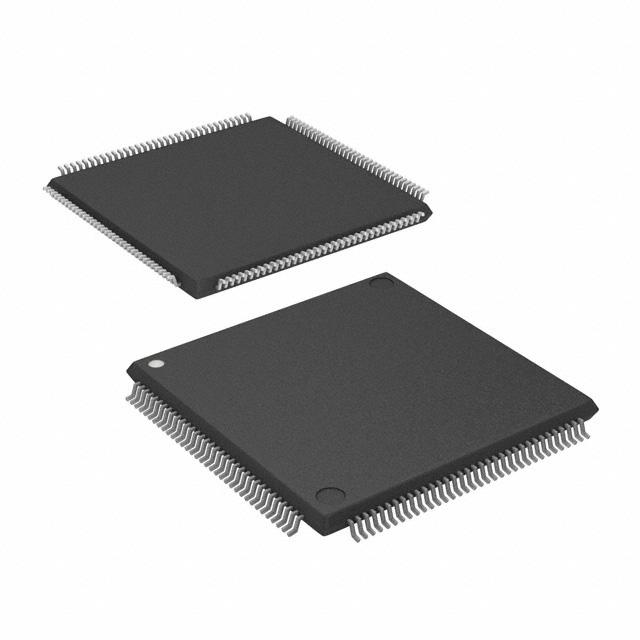
| Package / Case | 144-LQFP | |
| Supplier Device Package | 144-TQFP (20x20) | |
| Base Product Number | LFECP6 |
LFECP6E-3TN144C Datasheet Download
LFECP6E-3TN144C Overview
The LFECP6E-3TN144C is a low-power, high-performance Field Programmable Gate Array (FPGA) chip from Lattice Semiconductor Corporation. It is based on the LatticeECP3 architecture and is designed for applications requiring high-speed, low-power, and high-density logic.
The chip is available in a 144-pin package, and is compliant with the RoHS directive. It has a maximum operating frequency of 600 MHz and a maximum power dissipation of 3.3W. It also has an I/O voltage range of 1.2V to 3.3V.
The chip is equipped with 6,144 logic elements, 504 Kbits of RAM, and 184 I/O pins. It also has four phase-locked loops (PLLs) for clock synthesis and clock management. It also supports a wide range of I/O standards, including LVDS, LVCMOS, and SSTL.
The LFECP6E-3TN144C is suitable for a wide range of applications, including industrial automation, consumer electronics, automotive, communications, and networking. It is also suitable for applications requiring high-speed data transfer, low-power logic, and high-density logic.
You May Also Be Interested In
2,904 In Stock
Pricing (USD)
| QTY | Unit Price | Ext Price |
|---|---|---|
| No reference price found. | ||