

Lattice Semiconductor Corporation
LFECP6E-3QN208C
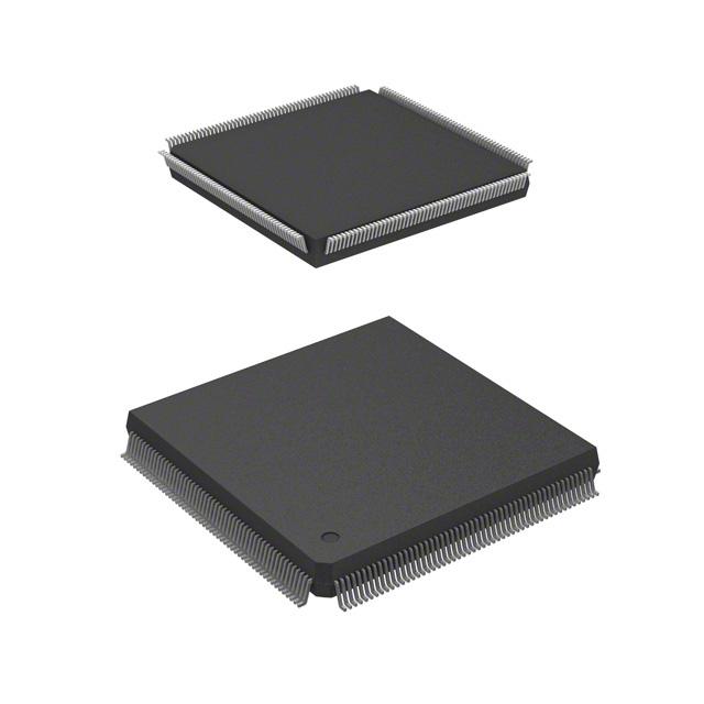
LFECP6E-3QN208C ECAD Model
LFECP6E-3QN208C Attributes
| Type | Description | Select |
|---|---|---|
| Mfr | Lattice Semiconductor Corporation | |
| Series | ECP | |
| Package | Tray | |
| Number of Logic Elements/Cells | 6100 | |
| Total RAM Bits | 94208 | |
| Number of I/O | 147 | |
| Voltage - Supply | 1.14V ~ 1.26V | |
| Mounting Type | Surface Mount | |
| Operating Temperature | 0°C ~ 85°C (TJ) | |
| Package / Case | 208-BFQFP | |
| Supplier Device Package | 208-PQFP (28x28) | |
| Base Product Number | LFECP6 |
LFECP6E-3QN208C Datasheet Download
LFECP6E-3QN208C Overview
The LFECP6E-3QN208C is a high-performance field-programmable gate array (FPGA) chip designed by Lattice Semiconductor Corporation. It is based on the company's low-power, low-cost, low-density, non-volatile FPGA technology. The chip is ideal for a wide range of applications, including the development of embedded systems, communications, industrial automation, medical imaging, and automotive applications.
The LFECP6E-3QN208C features an array of 3,208 logic cells, 4,096 Kbits of RAM, and an integrated phase-locked loop (PLL). It has a maximum power consumption of 1.4W and a maximum clock frequency of 250MHz. The chip also includes a wide range of I/O options, including LVDS, LVCMOS, and I2C, as well as a JTAG interface for programming and debugging.
The device is designed to provide a low-cost, low-power solution for embedded system designs. It is suitable for a wide range of applications, including automotive, industrial, medical, and communications applications. The device is also designed to be easy to use and program, making it an ideal choice for designers who need a reliable and cost-effective solution for their applications.
You May Also Be Interested In

2,457 In Stock
Pricing (USD)
| QTY | Unit Price | Ext Price |
|---|---|---|
| No reference price found. | ||