
Lattice Semiconductor Corporation
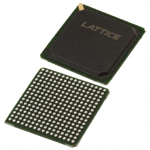
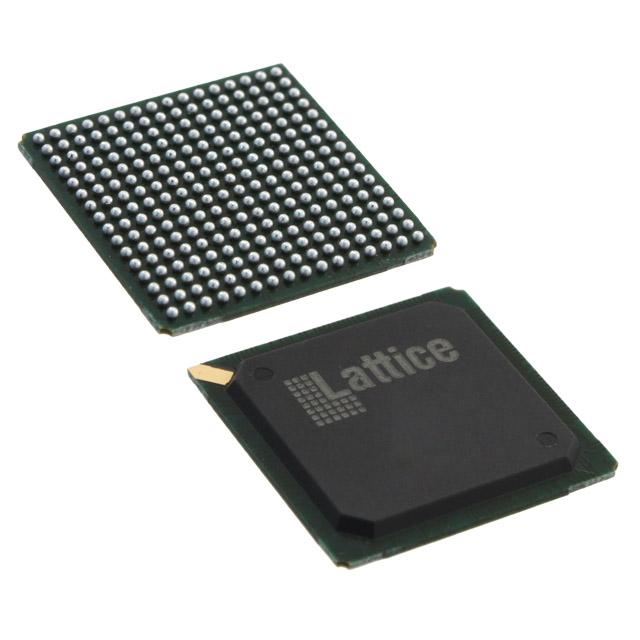
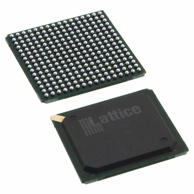
LFECP15E-5FN256C
LFECP15E-5FN256C ECAD Model
LFECP15E-5FN256C Attributes
| Type | Description | Select |
|---|---|---|
| Mfr | Lattice Semiconductor Corporation | |
| Series | ECP | |
| Package | Tray | |
| Number of Logic Elements/Cells | 15400 | |
| Total RAM Bits | 358400 | |
| Number of I/O | 195 | |
| Voltage - Supply | 1.14V ~ 1.26V | |
| Mounting Type | Surface Mount | |
| Operating Temperature | 0°C ~ 85°C (TJ) | |
| Package / Case | 256-BGA | |
| Supplier Device Package | 256-FPBGA (17x17) | |
| Base Product Number | LFECP15 |
LFECP15E-5FN256C Datasheet Download
LFECP15E-5FN256C Overview
The LFECP15E-5FN256C is a Field Programmable Gate Array (FPGA) chip manufactured by Lattice Semiconductor. It is a low-cost, low-power, high-performance FPGA chip that is suitable for a variety of applications.
The LFECP15E-5FN256C has a total of 256 logic cells and can support up to 28Kbits of RAM. It has a total of 8 I/O banks, each of which can support up to 48 I/O pins. The chip also features two dedicated clock outputs, two dedicated clock inputs, two dedicated clock enable pins, two dedicated clock enable outputs, two dedicated clock enable inputs, and two dedicated clock enable outputs.
The chip has a maximum operating frequency of 200 MHz and is capable of supporting up to 24 PLLs. It also has an integrated power management system and supports up to eight power islands. The chip also has an integrated on-chip debugging system.
The LFECP15E-5FN256C is suitable for a variety of applications such as communications, industrial automation, medical, automotive, and consumer electronics. It can be used for a variety of applications such as digital signal processing, image processing, video processing, and control systems.
Overall, the LFECP15E-5FN256C is a low-cost, low-power, high-performance FPGA chip that is suitable for a variety of applications. It has a total of 256 logic cells, 8 I/O banks, two dedicated clock outputs, two dedicated clock inputs, two dedicated clock enable pins, two dedicated clock enable outputs, two dedicated clock enable inputs, and two dedicated clock enable outputs. It also has an integrated power management system, supports up to 24 PLLs, and has an integrated on-chip debugging system.
You May Also Be Interested In
1,268 In Stock
Pricing (USD)
| QTY | Unit Price | Ext Price |
|---|---|---|
| No reference price found. | ||