
Lattice Semiconductor Corporation
LFECP10E-4F484I
LFECP10E-4F484I ECAD Model
LFECP10E-4F484I Attributes
| Type | Description | Select |
|---|---|---|
| Mfr | Lattice Semiconductor Corporation | |
| Series | ECP | |
| Package | Tray | |
| Number of Logic Elements/Cells | 10200 | |
| Total RAM Bits | 282624 | |
| Number of I/O | 288 | |
| Voltage - Supply | 1.14V ~ 1.26V | |
| Mounting Type | Surface Mount | |
| Operating Temperature | -40°C ~ 100°C (TJ) | |
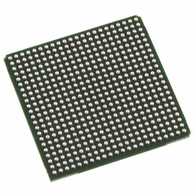
| Package / Case | 484-BBGA | |
| Supplier Device Package | 484-FPBGA (23x23) | |
| Base Product Number | LFECP10 |
LFECP10E-4F484I Overview
The LFECP10E-4F484I chip model is a low-power, low-cost Field Programmable Gate Array (FPGA) manufactured by Lattice Semiconductor Corporation. It is designed to provide a low-cost solution for embedded applications, such as industrial control, automotive, communications, and consumer electronics.
The LFECP10E-4F484I has an architecture that includes 4,484 logic elements, 10,240 flip-flops, and 4,096 RAM blocks. It is equipped with a 6-bit phase-locked loop (PLL) for clock management, and a high-speed, low-power transceiver for communication with external devices. The device also supports a wide range of I/O standards, including LVDS, LVCMOS, and SSTL.
The LFECP10E-4F484I is designed to operate at a maximum clock frequency of 200 MHz, and can be configured with up to four clock sources. It has a power consumption of 2.4 W, and a temperature range of -40°C to +85°C. The device also features advanced design features such as on-chip debugging, and a wide range of development tools.
The LFECP10E-4F484I is suitable for a variety of embedded applications, such as industrial control, automotive, communications, and consumer electronics. It is also well-suited for applications that require low power consumption and high performance. The device is also designed to provide a cost-effective solution for system designers.
You May Also Be Interested In
1,928 In Stock
Pricing (USD)
| QTY | Unit Price | Ext Price |
|---|---|---|
| No reference price found. | ||