
Lattice Semiconductor Corporation
LFEC3E-3TN144I
LFEC3E-3TN144I ECAD Model
LFEC3E-3TN144I Attributes
| Type | Description | Select |
|---|---|---|
| Mfr | Lattice Semiconductor Corporation | |
| Series | EC | |
| Package | Tray | |
| Number of Logic Elements/Cells | 3100 | |
| Total RAM Bits | 56320 | |
| Number of I/O | 97 | |
| Voltage - Supply | 1.14V ~ 1.26V | |
| Mounting Type | Surface Mount | |
| Operating Temperature | -40°C ~ 100°C (TJ) | |
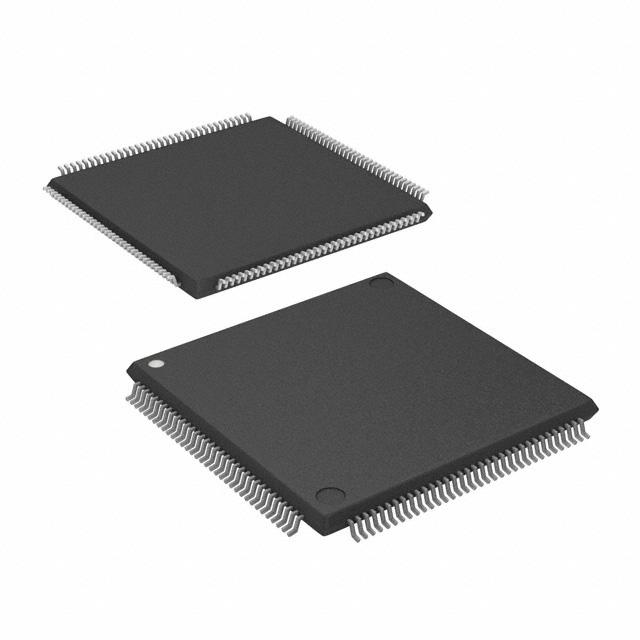
| Package / Case | 144-LQFP | |
| Supplier Device Package | 144-TQFP (20x20) | |
| Base Product Number | LFEC3 |
LFEC3E-3TN144I Datasheet Download
LFEC3E-3TN144I Overview
The LFEC3E-3TN144I is a Field Programmable Gate Array (FPGA) chip manufactured by Lattice Semiconductor Corporation. It is a low-cost, low-power, high-performance FPGA device that is ideal for a wide range of applications.
The LFEC3E-3TN144I features four independent, configurable logic blocks (CLBs) with 144 logic elements (LEs). It has a total of 24 I/O pins, with 12 of them being configurable as either single-ended or differential I/O. It also has two dedicated clock pins, with one being a global clock and the other being a dedicated clock input. The device is powered by a single 1.2V power supply and has a maximum operating frequency of 150MHz.
The LFEC3E-3TN144I is designed for applications such as embedded systems, industrial automation, machine vision, motor control, and digital signal processing. It offers a wide range of features, including low-power consumption, fast performance, and a high level of configurability. It also supports a variety of development tools, such as the Lattice Diamond design software and the Lattice Diamond Programmer.
Overall, the LFEC3E-3TN144I is an excellent choice for a wide variety of applications due to its low cost, low power consumption, and high performance. It is an ideal solution for developers looking for a reliable, cost-effective FPGA device.
You May Also Be Interested In
3,890 In Stock
Pricing (USD)
| QTY | Unit Price | Ext Price |
|---|---|---|
| No reference price found. | ||