
Lattice Semiconductor Corporation
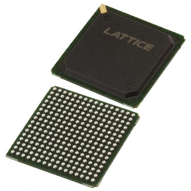
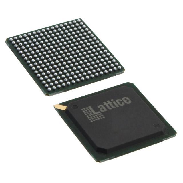
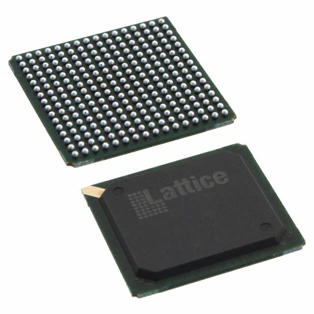
LFEC3E-3F256I
LFEC3E-3F256I ECAD Model
LFEC3E-3F256I Attributes
| Type | Description | Select |
|---|---|---|
| Mfr | Lattice Semiconductor Corporation | |
| Series | EC | |
| Package | Tray | |
| Number of Logic Elements/Cells | 3100 | |
| Total RAM Bits | 56320 | |
| Number of I/O | 160 | |
| Voltage - Supply | 1.14V ~ 1.26V | |
| Mounting Type | Surface Mount | |
| Operating Temperature | -40°C ~ 100°C (TJ) | |
| Package / Case | 256-BGA | |
| Supplier Device Package | 256-FPBGA (17x17) | |
| Base Product Number | LFEC3 |
LFEC3E-3F256I Datasheet Download
LFEC3E-3F256I Overview
The LFEC3E-3F256I is an FPGA chip model manufactured by Lattice Semiconductor Corporation. It is a low-power, low-cost, high-performance FPGA (Field Programmable Gate Array) device that provides a high level of flexibility and scalability. The device is designed to be used in a wide range of applications, including embedded systems, consumer electronics, automotive, industrial, and aerospace applications.
The LFEC3E-3F256I is a 3.3V device with a 256-bit internal configuration memory. It has a 5.5V tolerant I/O, and supports up to 12 I/O banks, providing up to 216 I/O pins. It has a maximum operating frequency of 300MHz, and can support up to 16,000 logic elements. The device also features a wide range of dedicated hardware resources, such as a dedicated DSP block, an embedded memory block, and a high-speed SERDES interface.
The LFEC3E-3F256I is a fully-featured FPGA device that provides a high level of flexibility and scalability. It is suitable for a wide range of applications, and can be used to create custom logic designs, control systems, and communication systems. The device is also suitable for use in high-speed data processing, image processing, and signal processing applications. It is also suitable for use in applications requiring low power consumption and low cost.
You May Also Be Interested In
1,616 In Stock
Pricing (USD)
| QTY | Unit Price | Ext Price |
|---|---|---|
| No reference price found. | ||