
Lattice Semiconductor Corporation
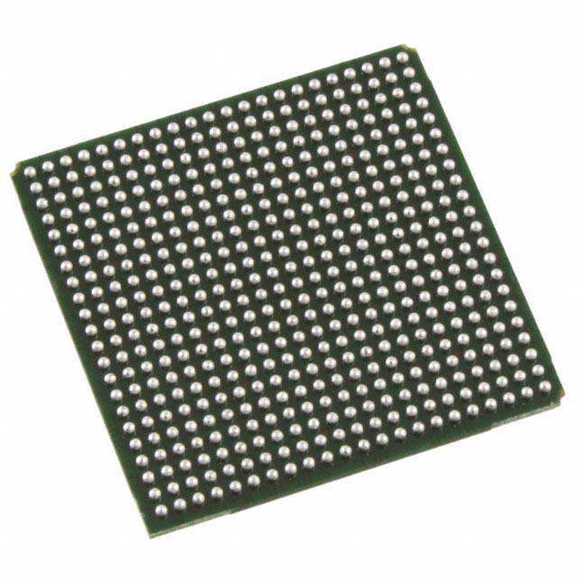
LFEC15E-4FN484I
LFEC15E-4FN484I ECAD Model
LFEC15E-4FN484I Attributes
| Type | Description | Select |
|---|---|---|
| Mfr | Lattice Semiconductor Corporation | |
| Series | EC | |
| Package | Tray | |
| Number of Logic Elements/Cells | 15400 | |
| Total RAM Bits | 358400 | |
| Number of I/O | 352 | |
| Voltage - Supply | 1.14V ~ 1.26V | |
| Mounting Type | Surface Mount | |
| Operating Temperature | -40°C ~ 100°C (TJ) | |
| Package / Case | 484-BBGA | |
| Supplier Device Package | 484-FPBGA (23x23) | |
| Base Product Number | LFEC15 |
LFEC15E-4FN484I Datasheet Download
LFEC15E-4FN484I Overview
The LFEC15E-4FN484I is an ultra-low-power, low-voltage, non-volatile field-programmable gate array (FPGA) chip designed by Lattice Semiconductor. This FPGA is ideal for applications that require low power consumption and high performance. It is available in a small, 4x4mm package, making it suitable for space-constrained designs.
The LFEC15E-4FN484I has a maximum speed of 150MHz and a maximum system clock frequency of 300MHz. It has a total of 4,096 logic elements and 484 user I/Os. It also features 4Kbits of SRAM, 8Kbits of EEPROM, and an integrated phase-locked loop (PLL). It is also capable of supporting up to 24 I/O banks and up to 32 I/O standards.
The LFEC15E-4FN484I is ideal for a wide range of applications, including automotive, consumer, industrial, and medical. It is suitable for applications such as motor control, digital signal processing, and wireless communication. It can also be used in medical devices such as medical imaging, patient monitoring, and medical diagnostic equipment. Additionally, it can be used in industrial applications such as industrial automation, process control, and machine vision.
In conclusion, the LFEC15E-4FN484I is an ultra-low-power, low-voltage, non-volatile FPGA chip designed by Lattice Semiconductor. It is suitable for a wide range of applications, including automotive, consumer, industrial, and medical. It features 4Kbits of SRAM, 8Kbits of EEPROM, and an integrated phase-locked loop (PLL). It is also capable of supporting up to 24 I/O banks and up to 32 I/O standards, making it an ideal choice for applications that require low power consumption and high performance.
You May Also Be Interested In
1,431 In Stock
Pricing (USD)
| QTY | Unit Price | Ext Price |
|---|---|---|
| No reference price found. | ||