
Lattice Semiconductor Corporation
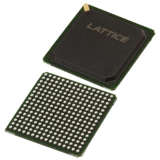
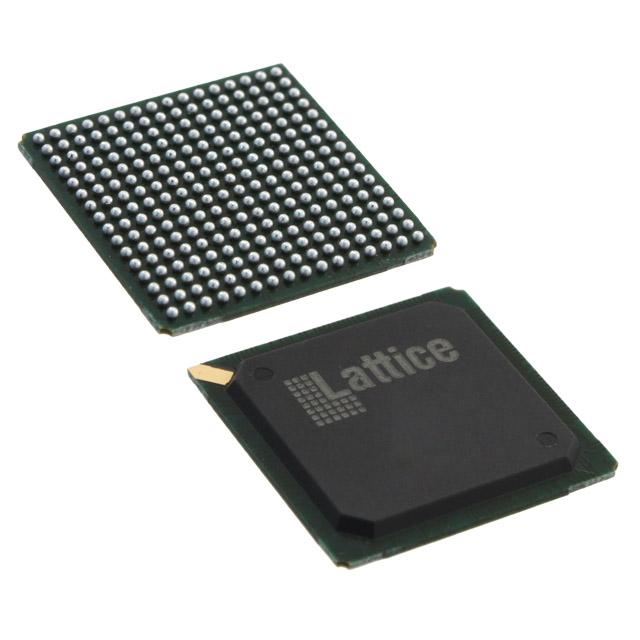
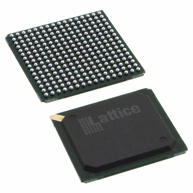
LFEC15E-3F256I
LFEC15E-3F256I ECAD Model
LFEC15E-3F256I Attributes
| Type | Description | Select |
|---|---|---|
| Mfr | Lattice Semiconductor Corporation | |
| Series | EC | |
| Package | Tray | |
| Number of Logic Elements/Cells | 15400 | |
| Total RAM Bits | 358400 | |
| Number of I/O | 195 | |
| Voltage - Supply | 1.14V ~ 1.26V | |
| Mounting Type | Surface Mount | |
| Operating Temperature | -40°C ~ 100°C (TJ) | |
| Package / Case | 256-BGA | |
| Supplier Device Package | 256-FPBGA (17x17) | |
| Base Product Number | LFEC15 |
LFEC15E-3F256I Overview
The LFEC15E-3F256I is a high-performance, low-power Field-Programmable Gate Array (FPGA) chip manufactured by Lattice Semiconductor. It is based on the LatticeECP3 FPGA family and is designed for applications requiring high levels of integration and flexibility.
The LFEC15E-3F256I has a total of 256Kbits of embedded SRAM and 3,840 logic elements. It also features 32 I/O pins, with support for up to four differential pairs. The chip is capable of operating at speeds up to 250 MHz and offers a total power dissipation of 1.5 watts.
The LFEC15E-3F256I is suitable for a variety of applications, including automotive, industrial, and consumer markets. It is designed to be used in high-performance, low-power applications such as motor control, power management, and sensor interfaces. It is also well suited for applications requiring high levels of integration, such as embedded systems, wireless communications, and digital signal processing.
The LFEC15E-3F256I is available in a range of packages, including TQFP, TFBGA, and VFBGA. It also offers a variety of features, including on-chip debugging, high-speed SERDES, and support for multiple voltage domains. The chip is also compatible with a variety of development tools, including the Lattice Diamond Design Suite, the Lattice Diamond Programmer, and the Lattice Diamond Analyzer.
You May Also Be Interested In
2,553 In Stock
Pricing (USD)
| QTY | Unit Price | Ext Price |
|---|---|---|
| No reference price found. | ||