
Lattice Semiconductor Corporation
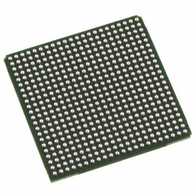
LFEC10E-4FN484I
LFEC10E-4FN484I ECAD Model
LFEC10E-4FN484I Attributes
| Type | Description | Select |
|---|---|---|
| Mfr | Lattice Semiconductor Corporation | |
| Series | EC | |
| Package | Tray | |
| Number of Logic Elements/Cells | 10200 | |
| Total RAM Bits | 282624 | |
| Number of I/O | 288 | |
| Voltage - Supply | 1.14V ~ 1.26V | |
| Mounting Type | Surface Mount | |
| Operating Temperature | -40°C ~ 100°C (TJ) | |
| Package / Case | 484-BBGA | |
| Supplier Device Package | 484-FPBGA (23x23) | |
| Base Product Number | LFEC10 |
LFEC10E-4FN484I Datasheet Download
LFEC10E-4FN484I Overview
The LFEC10E-4FN484I is a low-power, low-cost, field-programmable, gate array (FPGA) chip from Lattice Semiconductor. It is suitable for a wide range of applications, including industrial, automotive, consumer, medical, and communications applications.
The LFEC10E-4FN484I has a 4K logic cell capacity, with up to 484 I/O pins and a total of 2,048 configurable logic blocks (CLBs). It has up to 12.5Mb of SRAM, as well as support for multiple clock domains, allowing for high-speed operation. It also supports up to 28 LVDS channels and up to 8 LVDS pairs. The chip also has an integrated USB 2.0 PHY, as well as support for multiple protocols, including PCI Express, SPI, I2C, and UART.
The LFEC10E-4FN484I has an on-chip power management system, allowing for efficient power management. It also has an integrated JTAG interface, as well as support for a wide range of development tools, including the Lattice Diamond Design Suite and the Lattice Synthesis Tool.
In terms of applications, the LFEC10E-4FN484I is suitable for a wide range of applications, including industrial automation, automotive, consumer, medical, and communication applications. It can be used for applications such as motor control, power management, video processing, and networking.
In conclusion, the LFEC10E-4FN484I is a low-power, low-cost, field-programmable, gate array chip from Lattice Semiconductor. It is suitable for a wide range of applications, including industrial, automotive, consumer, medical, and communications applications. It has a 4K logic cell capacity, with up to 484 I/O pins and a total of 2,048 configurable logic blocks (CLBs). It also has an on-chip power management system, as well as support for multiple protocols, including PCI Express, SPI, I2C, and UART.
You May Also Be Interested In
1,465 In Stock
Pricing (USD)
| QTY | Unit Price | Ext Price |
|---|---|---|
| No reference price found. | ||