
Lattice Semiconductor Corporation
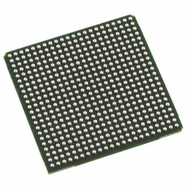
LFEC10E-3FN484I
LFEC10E-3FN484I ECAD Model
LFEC10E-3FN484I Attributes
| Type | Description | Select |
|---|---|---|
| Mfr | Lattice Semiconductor Corporation | |
| Series | EC | |
| Package | Tray | |
| Number of Logic Elements/Cells | 10200 | |
| Total RAM Bits | 282624 | |
| Number of I/O | 288 | |
| Voltage - Supply | 1.14V ~ 1.26V | |
| Mounting Type | Surface Mount | |
| Operating Temperature | -40°C ~ 100°C (TJ) | |
| Package / Case | 484-BBGA | |
| Supplier Device Package | 484-FPBGA (23x23) | |
| Base Product Number | LFEC10 |
LFEC10E-3FN484I Datasheet Download
LFEC10E-3FN484I Overview
The LFEC10E-3FN484I is a low-power, low-cost, high-performance field-programmable gate array (FPGA) chip from Lattice Semiconductor. It is designed to provide a flexible, cost-effective solution for a wide range of applications.
The LFEC10E-3FN484I is based on a 28nm process technology and features a 3.2V core voltage, a 0.8V I/O voltage, and a 4.8V I/O voltage. It has a total of 4,844 logic cells, 1,440 Flip-Flops, and 12,288 bits of RAM. It has a total of 484 I/O pins, with 4 banks of I/O pins, and a total of 10 I/O banks. It has a total of 8 DSP blocks, and a total of 6 Multiplier Blocks.
The LFEC10E-3FN484I is designed to provide high performance and low power consumption, making it suitable for a wide range of applications. It is suitable for applications such as embedded systems, industrial automation, data acquisition, medical electronics, automotive electronics, aerospace and defense, and consumer electronics.
The LFEC10E-3FN484I is designed to provide a cost-effective solution while still providing high performance and low power consumption. It is designed to be easy to use and program, making it suitable for a variety of applications. It is also designed to be reliable and robust, making it suitable for long-term use.
You May Also Be Interested In
3,425 In Stock
Pricing (USD)
| QTY | Unit Price | Ext Price |
|---|---|---|
| No reference price found. | ||