
Lattice Semiconductor Corporation
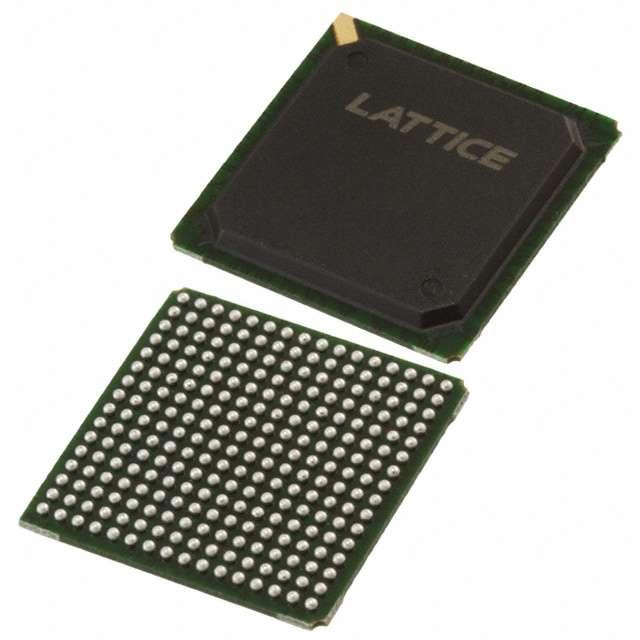
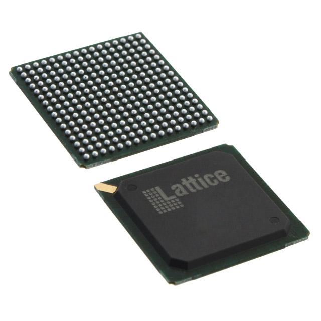
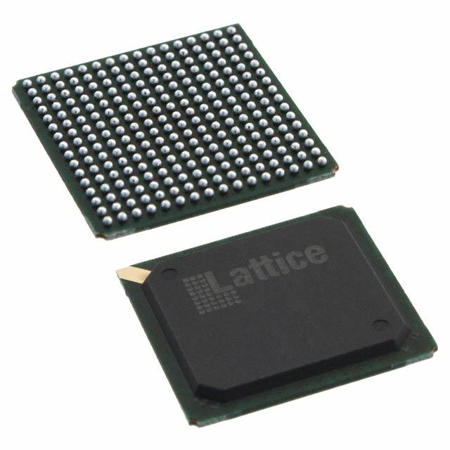
LFEC10E-3FN256I
LFEC10E-3FN256I ECAD Model
LFEC10E-3FN256I Attributes
| Type | Description | Select |
|---|---|---|
| Mfr | Lattice Semiconductor Corporation | |
| Series | EC | |
| Package | Tray | |
| Number of Logic Elements/Cells | 10200 | |
| Total RAM Bits | 282624 | |
| Number of I/O | 195 | |
| Voltage - Supply | 1.14V ~ 1.26V | |
| Mounting Type | Surface Mount | |
| Operating Temperature | -40°C ~ 100°C (TJ) | |
| Package / Case | 256-BGA | |
| Supplier Device Package | 256-FPBGA (17x17) | |
| Base Product Number | LFEC10 |
LFEC10E-3FN256I Datasheet Download
LFEC10E-3FN256I Overview
The LFEC10E-3FN256I is a low-power, low-voltage, 256-bit field-programmable gate array (FPGA) chip from Lattice Semiconductor. This chip is designed for high-performance and low-power applications in a variety of market segments, including consumer, industrial, automotive and medical.
The LFEC10E-3FN256I features an embedded memory of up to 256 bits, with a maximum clock frequency of up to 300 MHz. It is designed to operate at a voltage range of 1.2V to 3.3V, and provides an adjustable I/O drive strength of up to 8mA. The chip also features an on-chip voltage regulator, as well as low-power and high-speed operation modes.
The LFEC10E-3FN256I is ideal for applications that require both high-performance and low-power operation. It can be used for a variety of tasks, including image processing, signal processing, motion control, and embedded system design. Additionally, it is suitable for applications in consumer electronics, automotive, industrial, and medical segments.
The LFEC10E-3FN256I is designed for easy integration into any system, and it is highly reliable and cost-effective. It is available in a range of packages, including BGA, LQFP, and VFBGA. The chip is also RoHS compliant, and it is supported by a range of design tools and software.
You May Also Be Interested In
1,080 In Stock
Pricing (USD)
| QTY | Unit Price | Ext Price |
|---|---|---|
| No reference price found. | ||