
Lattice Semiconductor Corporation
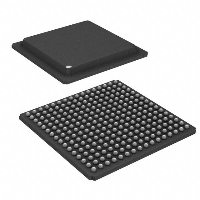
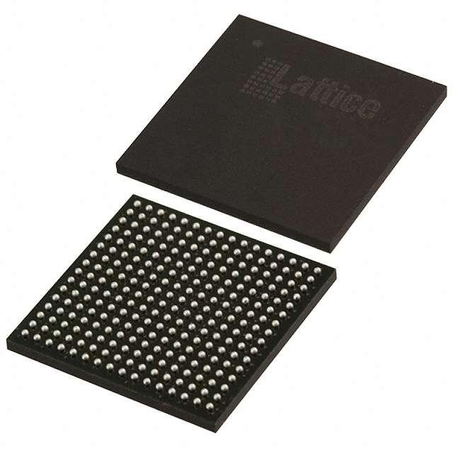
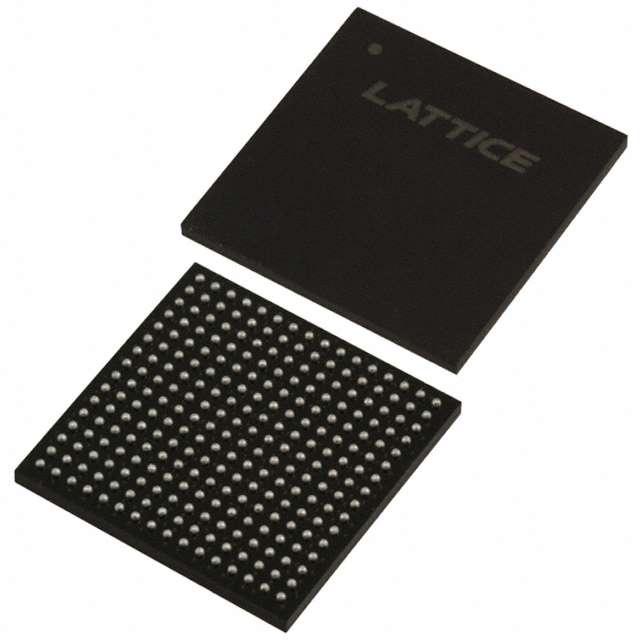
LFE3-35EA-6LFTN256I
LFE3-35EA-6LFTN256I ECAD Model
LFE3-35EA-6LFTN256I Attributes
| Type | Description | Select |
|---|---|---|
| Mfr | Lattice Semiconductor Corporation | |
| Series | ECP3 | |
| Package | Tray | |
| Number of LABs/CLBs | 4125 | |
| Number of Logic Elements/Cells | 33000 | |
| Total RAM Bits | 1358848 | |
| Number of I/O | 133 | |
| Voltage - Supply | 1.14V ~ 1.26V | |
| Mounting Type | Surface Mount | |
| Operating Temperature | -40°C ~ 100°C (TJ) | |
| Package / Case | 256-BGA | |
| Supplier Device Package | 256-FTBGA (17x17) | |
| Base Product Number | LFE3-35 |
LFE3-35EA-6LFTN256I Datasheet Download
LFE3-35EA-6LFTN256I Overview
The LFE3-35EA-6LFTN256I is a low-power, low-cost field-programmable gate array (FPGA) chip from Lattice Semiconductor. It is a member of the Lattice ECP3 family of FPGAs, which are built on the company’s advanced low-power, low-cost FPGA architecture.
The LFE3-35EA-6LFTN256I chip has a maximum operating frequency of 250 MHz and contains 256Kbits of internal memory. It has a total of 35K LEs (Logic Elements) and 1,872 Kbits of SRAM. It supports up to 8 user-defined I/O banks and up to 256 user-defined I/O pins. The chip is packaged in a 6mm x 6mm LQFP package, making it suitable for a variety of applications.
The LFE3-35EA-6LFTN256I chip is suitable for a wide range of applications, including embedded systems, industrial automation, medical imaging, motor control, and consumer electronics. It can be used to develop a wide range of applications, including digital signal processing, video processing, motor control, and image processing. It is also suitable for low-power, low-cost applications such as automotive, wearables, and IoT devices.
The LFE3-35EA-6LFTN256I chip is designed to reduce power consumption and cost while providing high performance. It features advanced power-saving technologies such as low-power I/O, low-power SRAM, and low-power logic. It also features advanced security features such as secure boot and secure debug.
In summary, the LFE3-35EA-6LFTN256I is a low-power, low-cost FPGA chip from Lattice Semiconductor. It has a maximum operating frequency of 250 MHz and contains 256Kbits of internal memory. It is suitable for a wide range of applications, including embedded systems, industrial automation, medical imaging, motor control, and consumer electronics. It also features advanced power-saving technologies and security features.
You May Also Be Interested In
5,200 In Stock
Pricing (USD)
| QTY | Unit Price | Ext Price |
|---|---|---|
| 1+ | $58.1750 | $58.1750 |
| 10+ | $57.5495 | $575.4950 |
| 100+ | $54.4218 | $5,442.1806 |
| 1000+ | $51.2941 | $25,647.0580 |
| 10000+ | $46.9154 | $46,915.3500 |
| The price is for reference only, please refer to the actual quotation! | ||