
Lattice Semiconductor Corporation
LFE3-35EA-6FN484I
LFE3-35EA-6FN484I ECAD Model
LFE3-35EA-6FN484I Attributes
| Type | Description | Select |
|---|---|---|
| Mfr | Lattice Semiconductor Corporation | |
| Series | ECP3 | |
| Package | Tray | |
| Number of LABs/CLBs | 4125 | |
| Number of Logic Elements/Cells | 33000 | |
| Total RAM Bits | 1358848 | |
| Number of I/O | 295 | |
| Voltage - Supply | 1.14V ~ 1.26V | |
| Mounting Type | Surface Mount | |
| Operating Temperature | -40°C ~ 100°C (TJ) | |
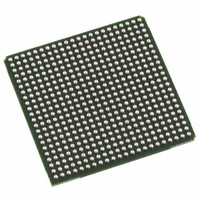
| Package / Case | 484-BBGA | |
| Supplier Device Package | 484-FPBGA (23x23) | |
| Base Product Number | LFE3-35 |
LFE3-35EA-6FN484I Datasheet Download
LFE3-35EA-6FN484I Overview
The LFE3-35EA-6FN484I is a low-power, high-performance, field-programmable gate array (FPGA) chip from Altera. It is designed for applications requiring high-speed signal processing, and features a wide range of features and capabilities.
The LFE3-35EA-6FN484I is constructed with a 6-layer metal programmable logic fabric and includes up to 6,784 logic elements and up to 6,784 flip-flops. It also offers up to 8,192 Kbits of embedded memory, up to 8,192 user I/Os, and up to 1,024 user-defined I/Os. Additionally, this chip has the ability to support up to two independent clock domains, and offers up to 1,024 total user-defined I/Os.
The LFE3-35EA-6FN484I is designed for applications requiring high-speed signal processing, such as communications, networking, imaging, and digital signal processing. It is also suitable for applications requiring high-density logic, such as embedded systems, industrial automation, and instrumentation.
In terms of power consumption, the LFE3-35EA-6FN484I operates at 3.3V and consumes a maximum of 2.5W of power. It also features a wide range of features and capabilities, such as error correction code (ECC), phase-locked loop (PLL), and clock management.
Overall, the LFE3-35EA-6FN484I is a low-power, high-performance FPGA chip that is suitable for a wide range of applications requiring high-speed signal processing. It is designed with a 6-layer metal programmable logic fabric, up to 8,192 Kbits of embedded memory, and up to 8,192 user I/Os, making it a powerful and versatile solution for a wide range of applications.
You May Also Be Interested In
1,936 In Stock
Pricing (USD)
| QTY | Unit Price | Ext Price |
|---|---|---|
| 1+ | $38.3161 | $38.3161 |
| 10+ | $37.9041 | $379.0409 |
| 100+ | $35.8441 | $3,584.4087 |
| 1000+ | $33.7841 | $16,892.0410 |
| 10000+ | $30.9001 | $30,900.0750 |
| The price is for reference only, please refer to the actual quotation! | ||