
Lattice Semiconductor Corporation
LFE3-17EA-8FTN256I
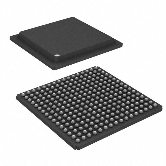
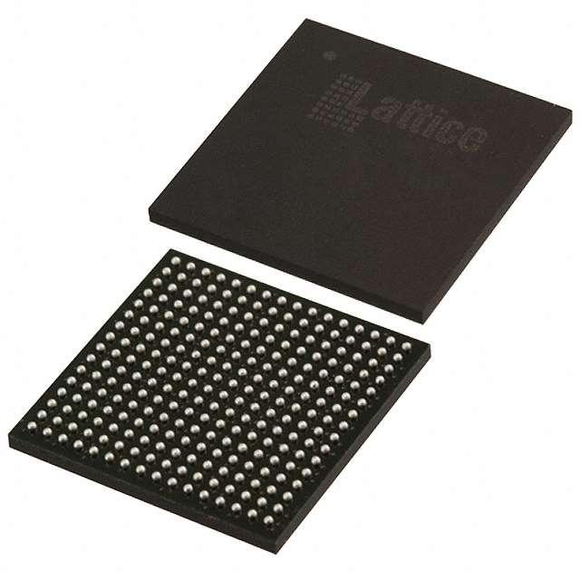
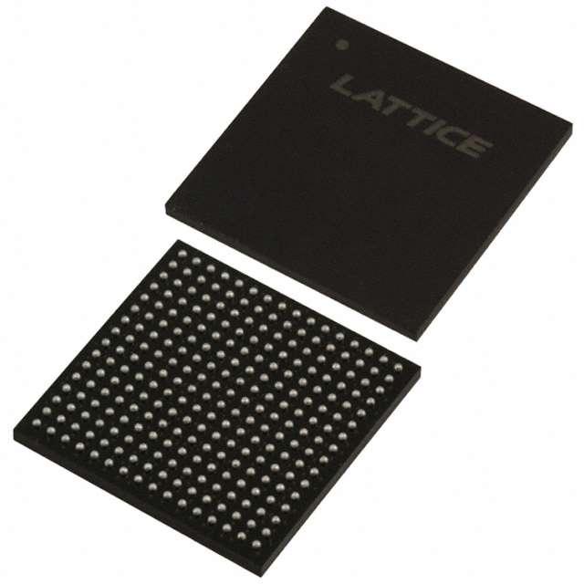
LFE3-17EA-8FTN256I ECAD Model
LFE3-17EA-8FTN256I Attributes
| Type | Description | Select |
|---|---|---|
| Mfr | Lattice Semiconductor Corporation | |
| Series | ECP3 | |
| Package | Tray | |
| Number of LABs/CLBs | 2125 | |
| Number of Logic Elements/Cells | 17000 | |
| Total RAM Bits | 716800 | |
| Number of I/O | 133 | |
| Voltage - Supply | 1.14V ~ 1.26V | |
| Mounting Type | Surface Mount | |
| Operating Temperature | -40°C ~ 100°C (TJ) | |
| Package / Case | 256-BGA | |
| Supplier Device Package | 256-FTBGA (17x17) | |
| Base Product Number | LFE3-17 |
LFE3-17EA-8FTN256I Datasheet Download
LFE3-17EA-8FTN256I Overview
The LFE3-17EA-8FTN256I is a low-power, high-performance, field-programmable gate array (FPGA) chip from Lattice Semiconductor. It is designed for use in a wide range of applications, including industrial, automotive, communications and consumer electronics.
The LFE3-17EA-8FTN256I is a mid-range FPGA chip, offering up to 17,500 logic cells and 256 Kbits of embedded memory. It supports up to 8 user-defined I/O banks, with up to 200 user-defined I/O pins. The chip also supports up to 8 global clock networks, with up to 6 high-speed SERDES channels.
The LFE3-17EA-8FTN256I is designed for low power consumption, with an active power consumption of 1.2 W and a standby power consumption of 0.3 W. It is also designed for high performance, with a maximum clock rate of 500 MHz and a maximum operating frequency of 300 MHz.
The LFE3-17EA-8FTN256I is suitable for a wide range of applications, including industrial control, automotive, communications, consumer electronics, medical and military applications. It is also suitable for applications requiring high speed and low power consumption, such as communications, networking, storage and embedded systems.
In summary, the LFE3-17EA-8FTN256I is a low-power, high-performance FPGA chip from Lattice Semiconductor, suitable for a wide range of applications. It offers up to 17,500 logic cells and 256 Kbits of embedded memory, with up to 8 user-defined I/O banks and 200 user-defined I/O pins. It also supports up to 8 global clock networks, with up to 6 high-speed SERDES channels. The chip is designed for low power consumption and high performance, with a maximum clock rate of 500 MHz and a maximum operating frequency of 300 MHz.
You May Also Be Interested In
5,013 In Stock
Pricing (USD)
| QTY | Unit Price | Ext Price |
|---|---|---|
| 1+ | $25.9286 | $25.9286 |
| 10+ | $25.6498 | $256.4978 |
| 100+ | $24.2558 | $2,425.5774 |
| 1000+ | $22.8618 | $11,430.8820 |
| 10000+ | $20.9102 | $20,910.1500 |
| The price is for reference only, please refer to the actual quotation! | ||