
Lattice Semiconductor Corporation
LFE3-17EA-7MG328I
LFE3-17EA-7MG328I ECAD Model
LFE3-17EA-7MG328I Attributes
| Type | Description | Select |
|---|---|---|
| Mfr | Lattice Semiconductor Corporation | |
| Series | ECP3 | |
| Package | Tray | |
| Number of LABs/CLBs | 2125 | |
| Number of Logic Elements/Cells | 17000 | |
| Total RAM Bits | 716800 | |
| Number of I/O | 116 | |
| Voltage - Supply | 1.14V ~ 1.26V | |
| Mounting Type | Surface Mount | |
| Operating Temperature | -40°C ~ 100°C (TJ) | |
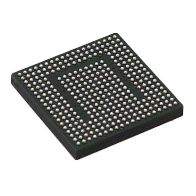
| Package / Case | 328-LFBGA, CSBGA | |
| Supplier Device Package | 328-CSBGA (10x10) | |
| Base Product Number | LFE3-17 |
LFE3-17EA-7MG328I Datasheet Download
LFE3-17EA-7MG328I Overview
The LFE3-17EA-7MG328I is a Field Programmable Gate Array (FPGA) chip model developed by Lattice Semiconductor. It is a 28nm FPGA with a low-power, low-cost, and high-performance architecture. It has 17K logic elements, 8Mb of embedded memory, and 576 I/O pins. The chip is optimized for high-speed serial connectivity, and features integrated transceivers, SERDES, and LVDS I/O. It is suitable for a wide range of applications, including industrial automation, medical imaging, wireless communications, and networking.
The chip is capable of providing a high-speed, low-power solution for applications that require high-speed data transfer, such as video streaming and high-speed data acquisition. It can also be used for high-speed serial communications, such as Ethernet and USB. The chip has a wide range of features, including on-chip analog-to-digital converters, on-chip clock management, and on-chip power management. It also supports multiple clock domains, allowing for clock synchronization and power management.
The chip is designed to be used in a variety of applications, from industrial automation and medical imaging to wireless communications and networking. It is also suitable for use in automotive, consumer, and IoT applications. The chip is designed to be compatible with a wide range of development tools and software, including the Lattice Diamond Design Suite, the Lattice Diamond Programmer, and the Lattice Diamond Simulator. The chip is also compatible with third-party development tools, such as the Xilinx Vivado Design Suite.
Overall, the LFE3-17EA-7MG328I is a versatile, low-power and high-performance FPGA chip model that is suitable for a wide range of applications. It is designed to provide a low-cost, high-speed solution for applications requiring high-speed data transfer, as well as a wide range of features and compatibility with a variety of development tools and software.
You May Also Be Interested In
5,526 In Stock
Pricing (USD)
| QTY | Unit Price | Ext Price |
|---|---|---|
| 1+ | $29.7636 | $29.7636 |
| 10+ | $29.4436 | $294.4359 |
| 100+ | $27.8434 | $2,784.3393 |
| 1000+ | $26.2432 | $13,121.5990 |
| 10000+ | $24.0029 | $24,002.9250 |
| The price is for reference only, please refer to the actual quotation! | ||