
Lattice Semiconductor Corporation
LFE2-6SE-7TN144C
LFE2-6SE-7TN144C ECAD Model
LFE2-6SE-7TN144C Attributes
| Type | Description | Select |
|---|---|---|
| Mfr | Lattice Semiconductor Corporation | |
| Series | ECP2 | |
| Package | Tray | |
| Number of LABs/CLBs | 750 | |
| Number of Logic Elements/Cells | 6000 | |
| Total RAM Bits | 56320 | |
| Number of I/O | 90 | |
| Voltage - Supply | 1.14V ~ 1.26V | |
| Mounting Type | Surface Mount | |
| Operating Temperature | 0°C ~ 85°C (TJ) | |
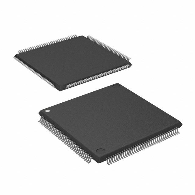
| Package / Case | 144-LQFP | |
| Supplier Device Package | 144-TQFP (20x20) | |
| Base Product Number | LFE2-6 |
LFE2-6SE-7TN144C Datasheet Download
LFE2-6SE-7TN144C Overview
The LFE2-6SE-7TN144C is a low-power, low-voltage, field-programmable gate array (FPGA) chip designed by Lattice Semiconductor. It is a member of the MachXO2 family of FPGAs and offers a wide range of features, including low power consumption and a small form factor. The chip has a total of 144 logic cells, 6 I/O banks, and 7Kbits of embedded memory. It is rated for a maximum operating voltage of 1.2V and a maximum operating temperature of 85°C.
The chip is ideal for applications that require low power consumption and a small form factor. It is suitable for use in a wide range of embedded systems, such as consumer electronics, industrial automation, medical devices, automotive systems, and more. The chip has built-in features such as support for multiple I/O standards, a wide range of clock frequencies, and a wide range of I/O voltages. It also has a wide range of configuration options, including the ability to configure up to 8 I/O banks and up to 48 logic cells.
In addition to its low power consumption and small form factor, the LFE2-6SE-7TN144C also offers a range of features that make it suitable for use in a variety of embedded applications. It has a wide range of I/O functions, including support for LVDS, LVCMOS, and HSTL. It also has a wide range of clock frequencies and I/O voltages. The chip also has built-in features such as a watchdog timer, a real-time clock, and an on-chip oscillator.
The LFE2-6SE-7TN144C is a versatile, low-power, low-voltage FPGA chip that is suitable for use in a wide range of embedded systems. It offers a wide range of features, including low power consumption, a small form factor, and a wide range of I/O functions. It is ideal for applications that require low power consumption and a small form factor.
You May Also Be Interested In
2,231 In Stock
Pricing (USD)
| QTY | Unit Price | Ext Price |
|---|---|---|
| 1+ | $18.9477 | $18.9477 |
| 10+ | $18.7440 | $187.4399 |
| 100+ | $17.7253 | $1,772.5293 |
| 1000+ | $16.7066 | $8,353.2990 |
| 10000+ | $15.2804 | $15,280.4250 |
| The price is for reference only, please refer to the actual quotation! | ||