
Lattice Semiconductor Corporation
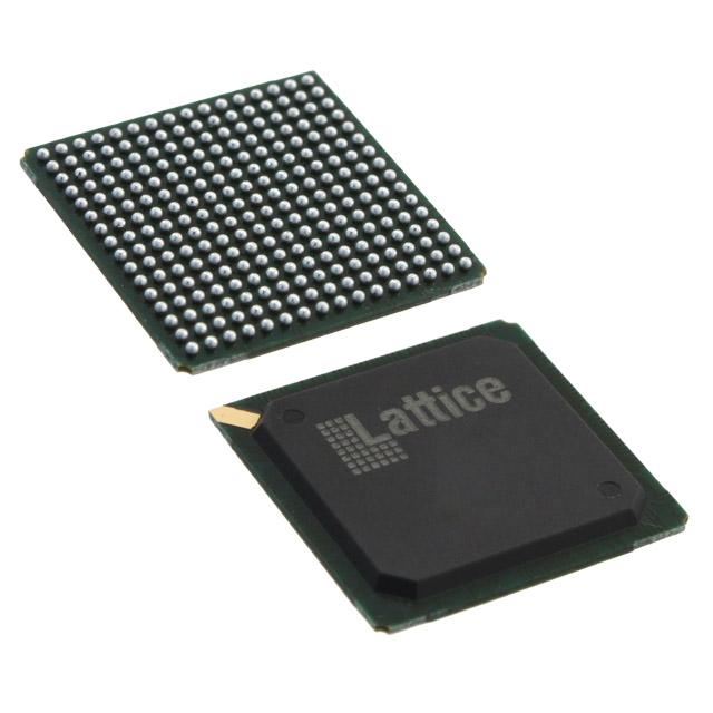
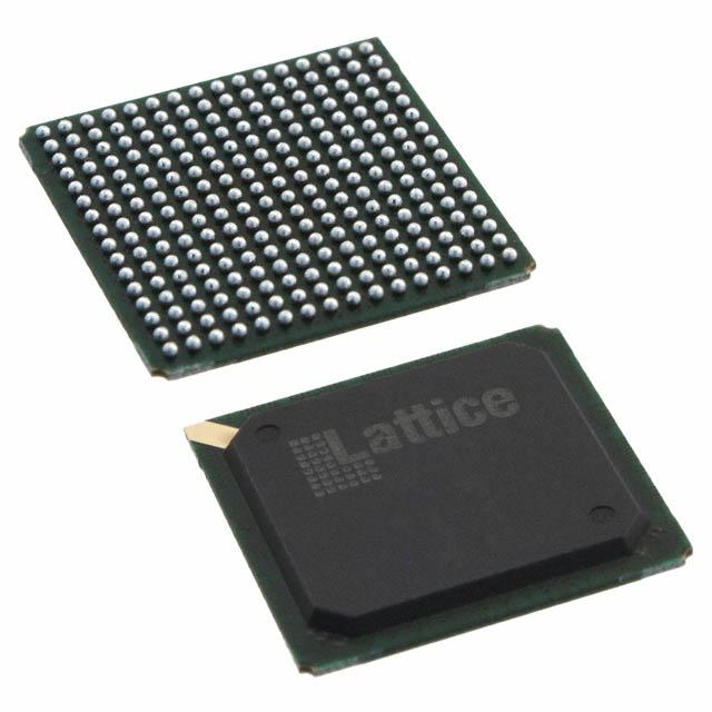
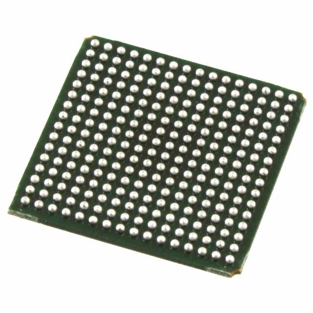
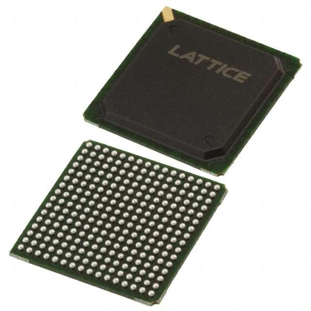
LFE2-6E-5FN256I
LFE2-6E-5FN256I ECAD Model
LFE2-6E-5FN256I Attributes
| Type | Description | Select |
|---|---|---|
| Mfr | Lattice Semiconductor Corporation | |
| Series | ECP2 | |
| Package | Tray | |
| Number of LABs/CLBs | 750 | |
| Number of Logic Elements/Cells | 6000 | |
| Total RAM Bits | 56320 | |
| Number of I/O | 190 | |
| Voltage - Supply | 1.14V ~ 1.26V | |
| Mounting Type | Surface Mount | |
| Operating Temperature | -40°C ~ 100°C (TJ) | |
| Package / Case | 256-BGA | |
| Supplier Device Package | 256-FPBGA (17x17) | |
| Base Product Number | LFE2-6 |
LFE2-6E-5FN256I Datasheet Download
LFE2-6E-5FN256I Overview
The LFE2-6E-5FN256I is an FPGA chip model from the Lattice Semiconductor Corporation. It is a low-power, low-cost, mid-range field programmable gate array (FPGA) chip that is suitable for a wide range of applications.
The LFE2-6E-5FN256I has a 6K logic cell array with up to 256-Kbits of embedded memory. It has a total of 576 I/O pins and can be configured to support a wide range of I/O standards, including LVDS, LVCMOS, HSTL, SSTL, and more. It also supports up to four banks of DDR2 and DDR3 memory.
The LFE2-6E-5FN256I is designed to be low-power and low-cost, making it suitable for a wide range of applications, including industrial automation, medical imaging, automotive, and consumer electronics. It is also suitable for applications where a high level of integration is required.
The LFE2-6E-5FN256I is a reliable and cost-effective FPGA chip model that can be used in a wide range of applications. It is designed to be low-power, low-cost, and highly integrated, making it suitable for a variety of applications.
You May Also Be Interested In
3,922 In Stock
Pricing (USD)
| QTY | Unit Price | Ext Price |
|---|---|---|
| 1+ | $15.1777 | $15.1777 |
| 10+ | $15.0145 | $150.1449 |
| 100+ | $14.1985 | $1,419.8487 |
| 1000+ | $13.3825 | $6,691.2410 |
| 10000+ | $12.2401 | $12,240.0750 |
| The price is for reference only, please refer to the actual quotation! | ||