
Lattice Semiconductor Corporation
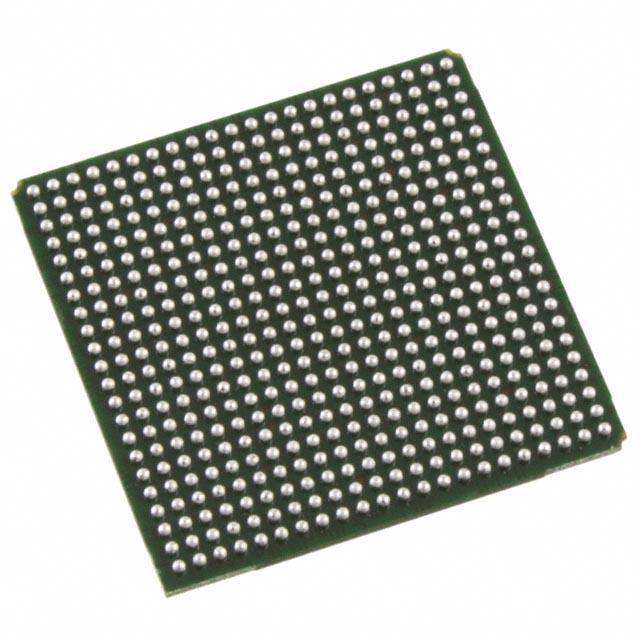
LFE2-50E-5F484C
LFE2-50E-5F484C ECAD Model
LFE2-50E-5F484C Attributes
| Type | Description | Select |
|---|---|---|
| Mfr | Lattice Semiconductor Corporation | |
| Series | ECP2 | |
| Package | Tray | |
| Number of LABs/CLBs | 6000 | |
| Number of Logic Elements/Cells | 48000 | |
| Total RAM Bits | 396288 | |
| Number of I/O | 339 | |
| Voltage - Supply | 1.14V ~ 1.26V | |
| Mounting Type | Surface Mount | |
| Operating Temperature | 0°C ~ 85°C (TJ) | |
| Package / Case | 484-BBGA | |
| Supplier Device Package | 484-FPBGA (23x23) | |
| Base Product Number | LFE2-50 |
LFE2-50E-5F484C Datasheet Download
LFE2-50E-5F484C Overview
The LFE2-50E-5F484C is a FPGA (Field Programmable Gate Array) chip model from Lattice Semiconductor. It is a low-power, low-cost, low-density FPGA device that is ideal for cost-sensitive designs. It has a maximum of 50K logic elements, up to 576KB of embedded memory and up to 5,500 user I/Os. It offers a wide range of features including I/O flexibility, power management, and advanced clocking resources.
The LFE2-50E-5F484C is a low-cost, low-power FPGA device that is suitable for cost-sensitive applications. It has a maximum of 50K logic elements, up to 576KB of embedded memory and up to 5,500 user I/Os. It is ideal for applications such as consumer electronics, automotive, industrial, and medical applications. It supports a wide range of I/O voltage levels, including 1.2V, 1.5V, 2.5V, and 3.3V. It is also compliant with the LVDS (Low Voltage Differential Signaling) standard.
The LFE2-50E-5F484C is also equipped with advanced power management features such as Power Down, Power Up, and Reset. It also features advanced clocking resources such as PLLs (Phase-Locked Loops), DLLs (Delay-Locked Loops), and clock dividers. It supports up to 48 user-defined clock domains and up to 24 user-defined PLLs.
The LFE2-50E-5F484C is a versatile FPGA device that is suitable for a wide range of applications. It is ideal for cost-sensitive designs and is suitable for consumer electronics, automotive, industrial, and medical applications. Its low power consumption, advanced power management features, and wide range of I/O voltage levels make it an ideal choice for cost-sensitive designs.
You May Also Be Interested In
4,124 In Stock
Pricing (USD)
| QTY | Unit Price | Ext Price |
|---|---|---|
| No reference price found. | ||