
Lattice Semiconductor Corporation
LFE2-20SE-5FN256C
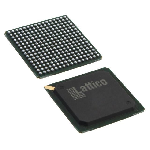
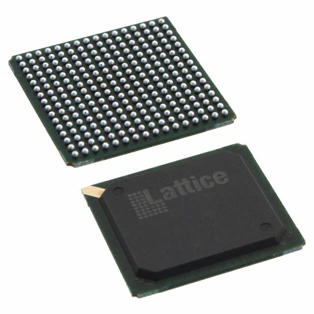
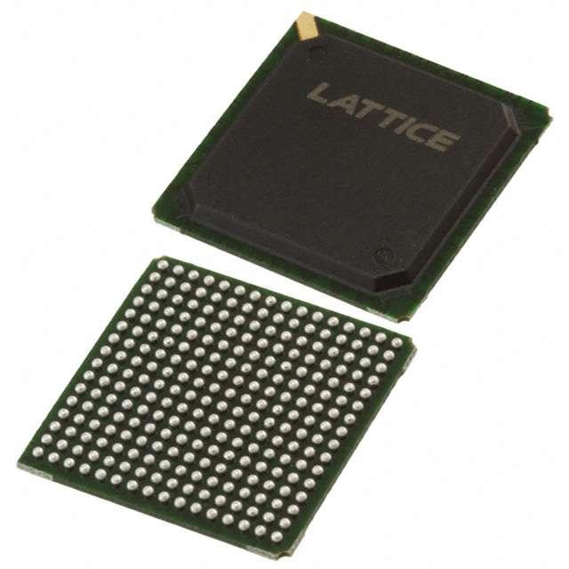
LFE2-20SE-5FN256C ECAD Model
LFE2-20SE-5FN256C Attributes
| Type | Description | Select |
|---|---|---|
| Mfr | Lattice Semiconductor Corporation | |
| Series | ECP2 | |
| Package | Tray | |
| Number of LABs/CLBs | 2625 | |
| Number of Logic Elements/Cells | 21000 | |
| Total RAM Bits | 282624 | |
| Number of I/O | 193 | |
| Voltage - Supply | 1.14V ~ 1.26V | |
| Mounting Type | Surface Mount | |
| Operating Temperature | 0°C ~ 85°C (TJ) | |
| Package / Case | 256-BGA | |
| Supplier Device Package | 256-FPBGA (17x17) | |
| Base Product Number | LFE2-20 |
LFE2-20SE-5FN256C Datasheet Download
LFE2-20SE-5FN256C Overview
The LFE2-20SE-5FN256C is a low-cost, low-power, field-programmable gate array (FPGA) chip model manufactured by Lattice Semiconductor Corporation. It is based on the company’s low-power, low-cost, non-volatile FPGA technology. The chip is designed for applications requiring low power consumption, low cost, and high reliability. The LFE2-20SE-5FN256C has a total of 256 configurable logic blocks (CLBs) and a total of 20,000 logic elements (LEs). It also features 8,192 bits of RAM, 4,096 bits of distributed RAM, and 16 DSP blocks.
The chip is designed for a wide range of applications, such as communications, consumer, industrial, and automotive. It is suitable for applications requiring low power consumption, such as battery-powered devices, as well as for applications requiring high reliability, such as medical devices. The chip is also suitable for applications requiring high data rates, such as video processing.
The LFE2-20SE-5FN256C is designed to be used in a wide range of applications, including embedded systems, wireless systems, and industrial control. It is also suitable for applications requiring low power consumption, high reliability, and high data rates. The chip is available in a range of package sizes, including BGA, QFN, and TQFP. It is also available in a range of speed grades, from 6 to 12.
The LFE2-20SE-5FN256C is a low-cost, low-power, field-programmable gate array (FPGA) chip model manufactured by Lattice Semiconductor Corporation. It is designed for a wide range of applications, such as communications, consumer, industrial, and automotive, and is suitable for applications requiring low power consumption, high reliability, and high data rates. The chip has a total of 256 configurable logic blocks (CLBs) and a total of 20,000 logic elements (LEs), as well as 8,192 bits of RAM, 4,096 bits of distributed RAM, and 16 DSP blocks. It is available in a range of package sizes, including BGA, QFN, and TQFP, and in a range of speed grades, from 6 to 12.
You May Also Be Interested In
4,078 In Stock
Pricing (USD)
| QTY | Unit Price | Ext Price |
|---|---|---|
| 1+ | $49.5897 | $49.5897 |
| 10+ | $49.0565 | $490.5652 |
| 100+ | $46.3904 | $4,639.0401 |
| 1000+ | $43.7243 | $21,862.1430 |
| 10000+ | $39.9917 | $39,991.7250 |
| The price is for reference only, please refer to the actual quotation! | ||