
Lattice Semiconductor Corporation
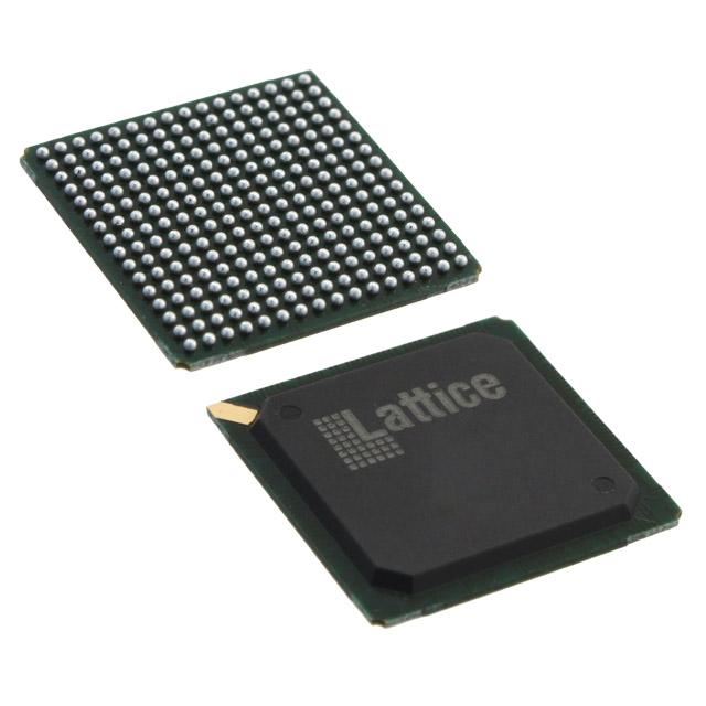
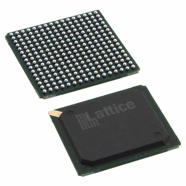
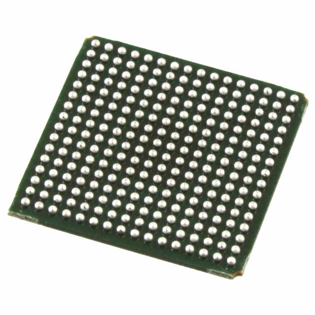
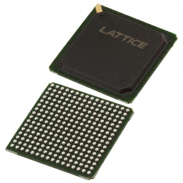
LFE2-12SE-7F256C
LFE2-12SE-7F256C ECAD Model
LFE2-12SE-7F256C Attributes
| Type | Description | Select |
|---|---|---|
| Mfr | Lattice Semiconductor Corporation | |
| Series | ECP2 | |
| Package | Tray | |
| Number of LABs/CLBs | 1500 | |
| Number of Logic Elements/Cells | 12000 | |
| Total RAM Bits | 226304 | |
| Number of I/O | 193 | |
| Voltage - Supply | 1.14V ~ 1.26V | |
| Mounting Type | Surface Mount | |
| Operating Temperature | 0°C ~ 85°C (TJ) | |
| Package / Case | 256-BGA | |
| Supplier Device Package | 256-FPBGA (17x17) | |
| Base Product Number | LFE2-12 |
LFE2-12SE-7F256C Datasheet Download
LFE2-12SE-7F256C Overview
The LFE2-12SE-7F256C is a low-power FPGA chip from Lattice Semiconductor. It is a member of the MachXO2 family of FPGAs and is designed to deliver high performance, low cost and low power consumption. It is built on a 0.5μm process featuring up to 12K LUTs and up to 256Kbits of RAM. It has an operating voltage range of 1.2V to 3.3V and a maximum operating temperature of 85°C.
The LFE2-12SE-7F256C has a wide range of features including enhanced I/O, embedded flash memory, programmable logic, and low power operation. It has a total of 8 I/O banks, each with up to 24 I/O pins, and an embedded flash memory of up to 256Kbits. It also has an integrated SPI port and a JTAG port for programming and debugging. The LFE2-12SE-7F256C also features a low power standby mode, reducing power consumption to less than 10µW.
The LFE2-12SE-7F256C is suitable for a wide range of applications, such as consumer electronics, automotive, industrial, and communication systems. It can be used for a variety of tasks such as data acquisition, signal processing, image processing, control systems, and embedded system designs. It is also suitable for applications that require a low power, low cost, and high performance solution.
You May Also Be Interested In
1,855 In Stock
Pricing (USD)
| QTY | Unit Price | Ext Price |
|---|---|---|
| No reference price found. | ||