
Lattice Semiconductor Corporation
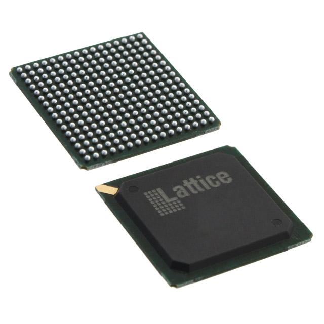
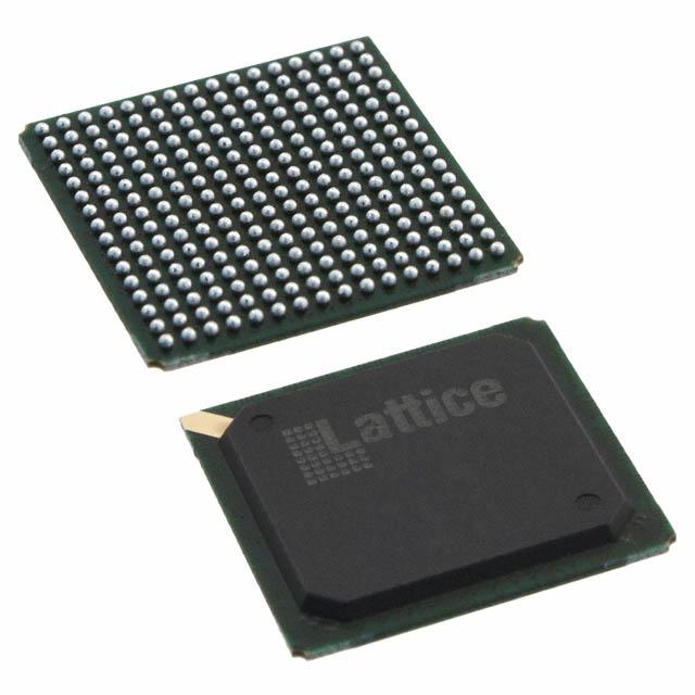
LFE2-12SE-6FN256I
LFE2-12SE-6FN256I ECAD Model
LFE2-12SE-6FN256I Attributes
| Type | Description | Select |
|---|---|---|
| Mfr | Lattice Semiconductor Corporation | |
| Series | ECP2 | |
| Package | Tray | |
| Number of LABs/CLBs | 1500 | |
| Number of Logic Elements/Cells | 12000 | |
| Total RAM Bits | 226304 | |
| Number of I/O | 193 | |
| Voltage - Supply | 1.14V ~ 1.26V | |
| Mounting Type | Surface Mount | |
| Operating Temperature | -40°C ~ 100°C (TJ) | |
| Package / Case | 256-BGA | |
| Supplier Device Package | 256-FPBGA (17x17) | |
| Base Product Number | LFE2-12 |
LFE2-12SE-6FN256I Datasheet Download
LFE2-12SE-6FN256I Overview
The LFE2-12SE-6FN256I is a low-power, low-cost, low-footprint FPGA chip from Lattice Semiconductor. It is designed for a range of applications such as industrial automation, consumer electronics, medical and automotive. It is an ultra-compact, low-power FPGA with a single-ended I/O voltage range of 1.2V to 3.3V. It is built with an advanced low-power, low-footprint architecture, making it suitable for space-constrained applications.
The chip has a total of 12,000 logic elements and 256Kbits of RAM, and can support up to 500 user-defined I/O pins. It has a maximum operating frequency of 250MHz, and a maximum clock-to-output delay of 4.7ns. It also features a built-in Phase Locked Loop (PLL) and a wide range of I/O features including differential I/O, LVDS, and LVCMOS.
The LFE2-12SE-6FN256I is designed for a wide range of applications, from industrial automation and consumer electronics to medical and automotive. It is especially useful for applications that require low-power and low-footprint solutions. It also has the capability to support multiple protocols such as Ethernet, USB, and CAN, making it suitable for a variety of applications.
In summary, the LFE2-12SE-6FN256I is a low-power, low-cost, low-footprint FPGA chip from Lattice Semiconductor. It is suitable for a range of applications and has a total of 12,000 logic elements and 256Kbits of RAM, a maximum operating frequency of 250MHz, and a maximum clock-to-output delay of 4.7ns. It also features a wide range of I/O features and supports multiple protocols, making it an ideal choice for space-constrained applications.
You May Also Be Interested In
1,370 In Stock
Pricing (USD)
| QTY | Unit Price | Ext Price |
|---|---|---|
| 1+ | $48.5045 | $48.5045 |
| 10+ | $47.9830 | $479.8297 |
| 100+ | $45.3752 | $4,537.5198 |
| 1000+ | $42.7674 | $21,383.7140 |
| 10000+ | $39.1166 | $39,116.5500 |
| The price is for reference only, please refer to the actual quotation! | ||